Fingerprint sensing device and fingerprint sensing method thereof

Inactive Publication Date: 2016-06-30
ELAN MICROELECTRONICS CORPORATION
View PDF1 Cites 20 Cited by
  • Summary
  • Abstract
  • Description
  • Claims
  • Application Information

AI Technical Summary

Benefits of technology

[0010]The present invention uses the shielding plate under the electrode plate to reduce the parasitic capacitor between the electrode plate and other conductors thereunder. Accordingly, a larger signal dynamic range can be achieved and the electrode plate can be preven

Problems solved by technology

Consequently, it will be more difficult to co

Method used


Image

  • Fingerprint sensing device and fingerprint sensing method thereof
  • Fingerprint sensing device and fingerprint sensing method thereof
  • Fingerprint sensing device and fingerprint sensing method thereof

Examples


Embodiment Construction

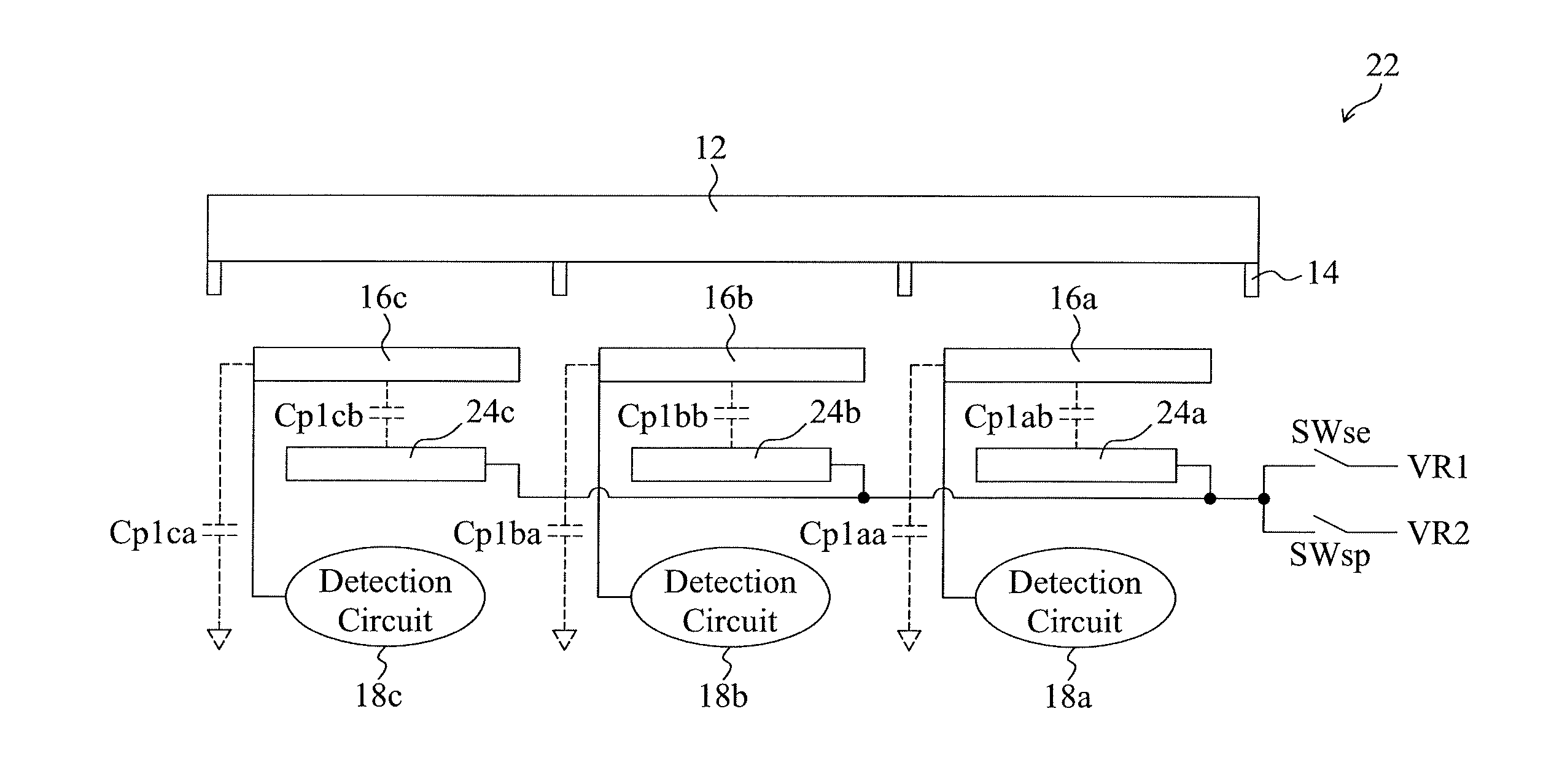
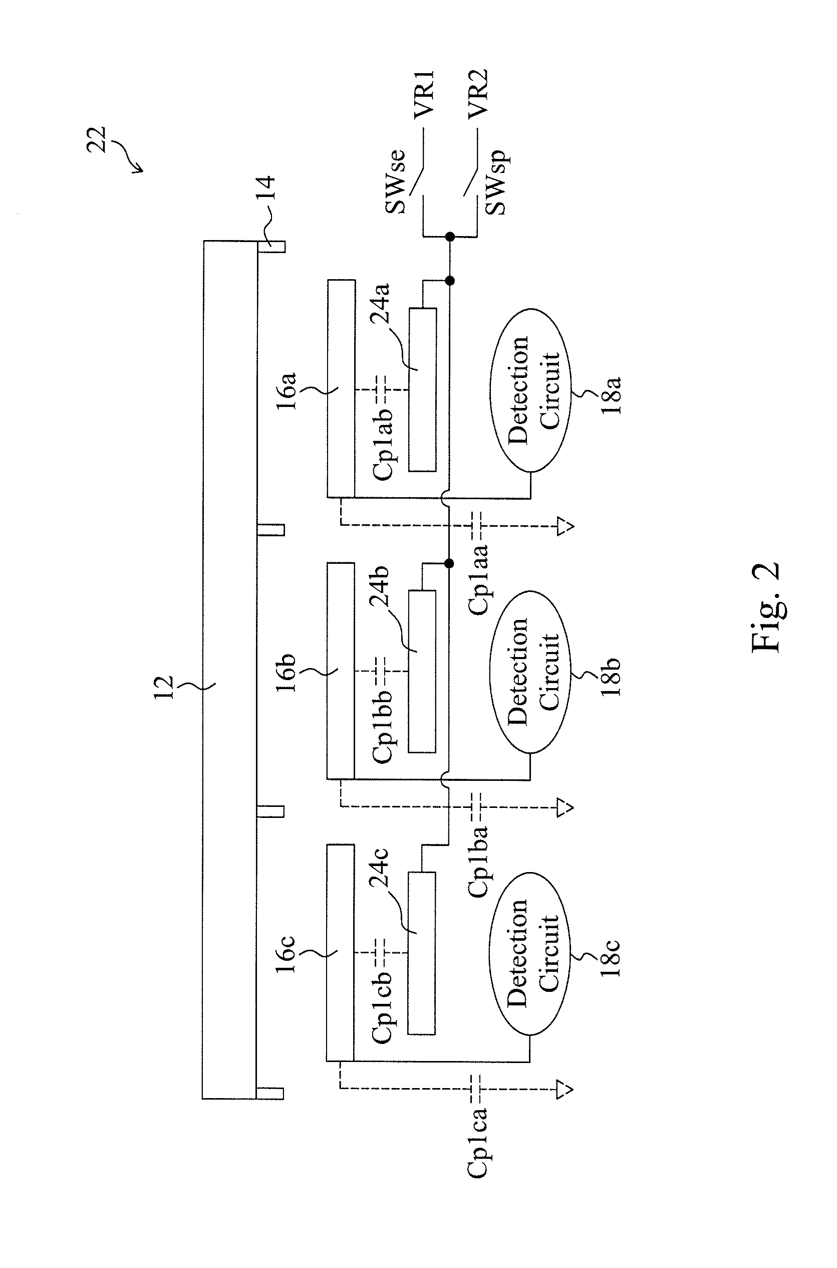
[0019]FIG. 2 shows an embodiment of a fingerprint sensing device 22 of the present invention, which comprises the similar protection layer 12, ESD layer 14, electrode plate 16a, 16b, and 16c, and detection circuits 18a, 18b, and 18c as those in the conventional fingerprint sensing device 10 in FIG. 1. Besides, the fingerprint sensing device 22 further comprises shielding plates 24a, 24b, and 24c, and switches SWse and SWsp. Wherein, the shielding plate 24a is configured between the electrode plate 16a and the detection circuit 18a. The shielding plate 24b is configured between the electrode plate 16b and the detection circuit 18b. The shielding plate 24c is configured between the electrode plate 16c and the detection circuit 18c. One terminal of the switch SWse is connected to the shielding plates 24a, 24b, and 24c. The other terminal of the switch SWse receives a voltage VR1. One terminal of the switch SWsp is connected to the shielding plates 24a, 24b, and 24c. The other terminal ...


PUM


Abstract

A fingerprint sensing device comprises a shielding plate configured between an electrode plate and a detection circuit for reducing a parasitic capacitor between the electrode plate and a conductor thereunder. Consequently, a larger signal dynamic range can be achieved and the electrode plate can be prevented from operation noise interference of the detection circuit. The shielding plate and the electrode plate have the same potential. Accordingly, a parasitic capacitor effect between the shielding plate and the electrode plate can be eliminated. Thus, the fingerprint sensing device of the present invention has a better noise resistibility.

Description

CROSS-REFERENCE TO RELATED APPLICATIONS[0001]This application claims priority benefit of U.S. Provisional Patent Application Ser. No. 62 / 096,894, filed Dec. 26, 2014, and Taiwan Patent Application No. 104139496, filed Nov. 26, 2015, which are hereby incorporated by reference in its entirety.FIELD OF THE INVENTION[0002]The present invention is related generally to a fingerprint sensing device and a method thereof, more particularly, to a low parasitic capacitance fingerprint sensing device and a fingerprint sensing method thereof.BACKGROUND OF THE INVENTION[0003]FIG. 1 shows a conventional fingerprint sensing device 10. A protection layer 12 is provided for fingers to touch and for protecting electrode plates 16a, 16b, and 16c thereunder. An electro-static discharge (ESD) layer 14 provides an ESD protection. Detection circuits 18a, 18b, and 18c are connected to the electrode plates 16a, 16b, and 16c, respectively, thereby detecting a capacitance value between the electrode plates 16a...

Claims


Application Information

Patent Timeline
IPC IPC(8): G06K9/00
CPCG06K9/0002G06V40/1306
Inventor YANG, CHAO-CHI
Owner ELAN MICROELECTRONICS CORPORATION
Why Eureka
Try Eureka