Confined early epitaxy with local interconnect capability

Active Publication Date: 2016-06-30
GLOBALFOUNDRIES US INC
View PDF0 Cites 3 Cited by
  • Summary
  • Abstract
  • Description
  • Claims
  • Application Information

AI Technical Summary

Benefits of technology

This patent describes a method and structure for improving contact resistivity in semiconductor devices. The method involves creating raised semiconductor structures surrounded by a layer of isolation material, and replacing them with dummy gates surrounded by hard mask material. This allows for the creation of confined epitaxial material above the active regions of the raised structures, which can help reduce contact resistivity. The resulting structure also includes non-planar semiconductor structures with replacement gate structures, silicide on the epitaxial material, and contacts on top of the silicide. Overall, this invention provides a way to improve the performance and reliability of semiconductor devices.

Problems solved by technology

For example, non-planar transistors using epitaxial semiconductor material for the source and drain would suffer inadequate size, in light of the vulnerability of the epitaxial material to fabrication processes (e.g., contact etches) and the resulting high resistance.
In addition, the inadequate size of the epitaxial material leaves inadequate area for silicide, and results in a contact resistivity that is too high.
Further, inadequately sized epitaxial material cannot simply be addressed by growing more epitaxial material, as that can lead to various device short failures, due to the narrow distance between devices and lateral growth of the epitaxial material.

Method used


Image

  • Confined early epitaxy with local interconnect capability
  • Confined early epitaxy with local interconnect capability
  • Confined early epitaxy with local interconnect capability

Examples


Embodiment Construction

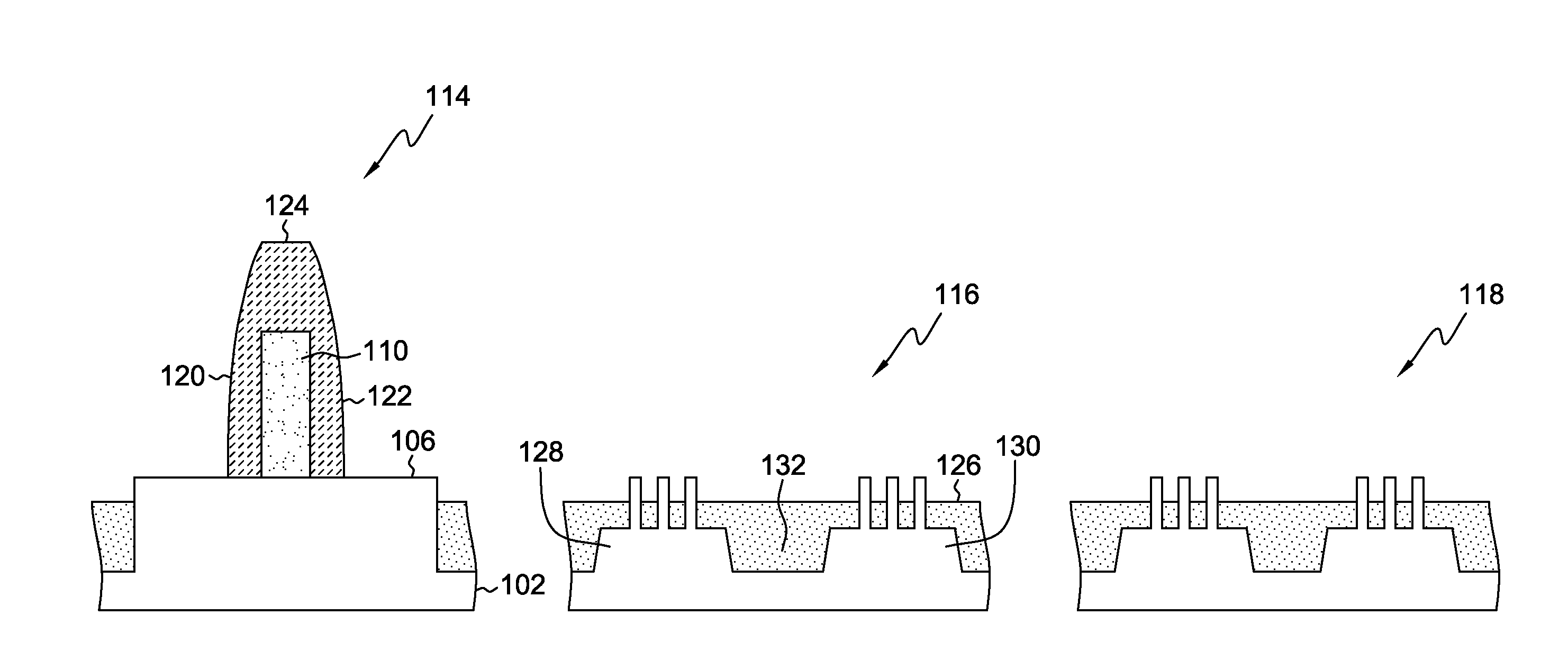
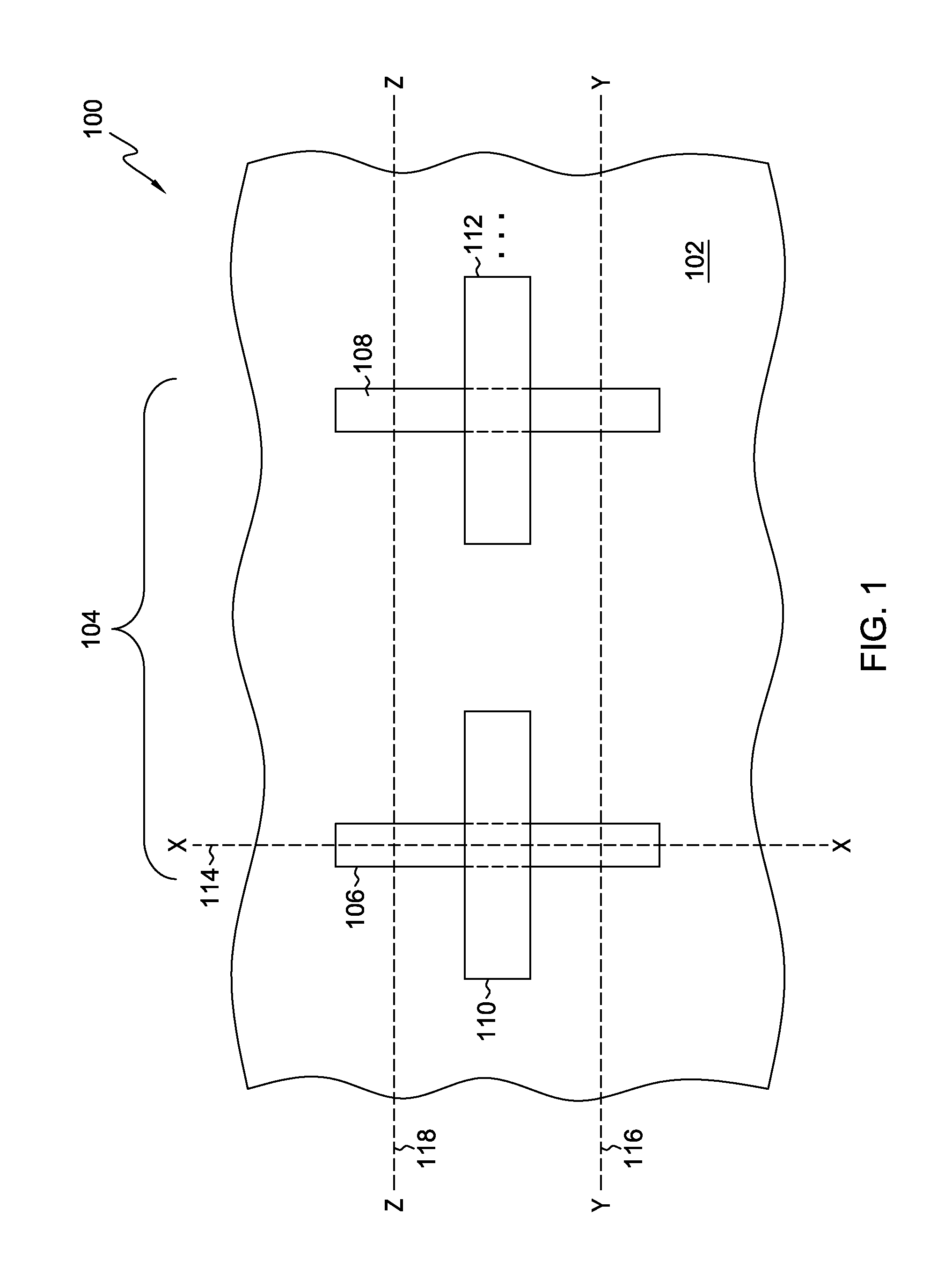
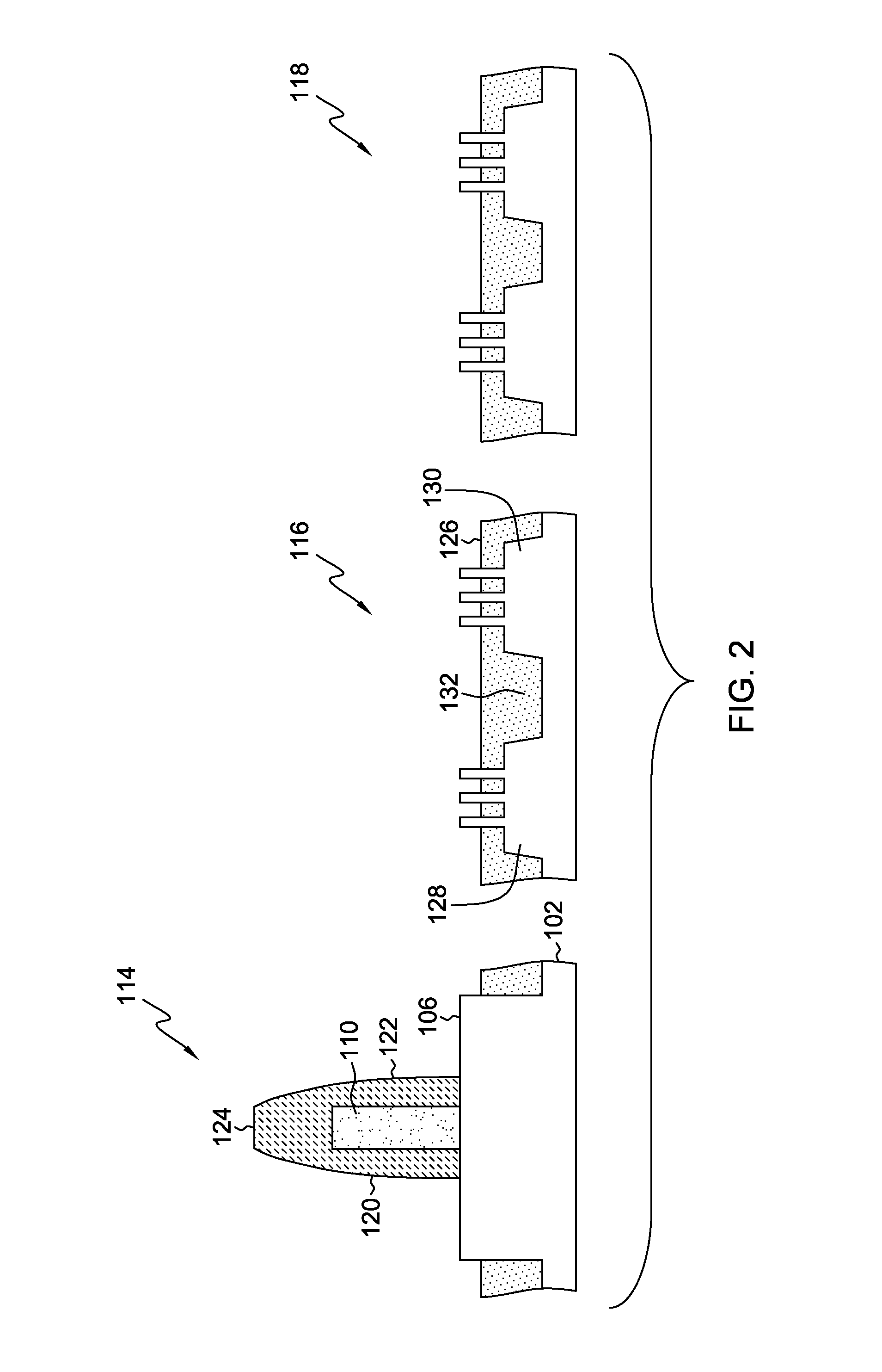
[0028]Aspects of the present invention and certain features, advantages, and details thereof, are explained more fully below with reference to the non-limiting examples illustrated in the accompanying drawings. Descriptions of well-known materials, fabrication tools, processing techniques, etc., are omitted so as not to unnecessarily obscure the invention in detail. It should be understood, however, that the detailed description and the specific examples, while indicating aspects of the invention, are given by way of illustration only, and are not by way of limitation. Various substitutions, modifications, additions, and / or arrangements, within the spirit and / or scope of the underlying inventive concepts will be apparent to those skilled in the art from this disclosure.

[0029]Approximating language, as used herein throughout the specification and claims, may be applied to modify any quantitative representation that could permissibly vary without resulting in a change in the basic fun...


PUM


Abstract

A non-planar semiconductor structure includes a semiconductor substrate, multiple raised semiconductor structures coupled to the substrate and surrounded at a lower portion thereof by a layer of isolation material, gate structure(s) and confined epitaxial material above active regions of the raised structures, the confined epitaxial material having recessed portion(s) therein. Dummy gate structures surrounding a portion of each of the raised structures are initially used, and the confined epitaxial material is created before replacing the dummy gate structures with final gate structures. The structure further includes silicide on upper surfaces of a top portion of the confined epitaxial material, and contacts above the silicide, the contacts including separate contacts electrically coupled to only one area of confined epitaxial material and common contact(s) electrically coupling two adjacent areas of the confined epitaxial material.

Description

BACKGROUND OF THE INVENTION[0001]1. Technical Field[0002]The present invention generally relates to contacts for semiconductor devices. More particularly, the present invention relates to contact structures and the use of confined epitaxial material for active regions of semiconductor devices.[0003]2. Background Information[0004]As overall semiconductor device size continues to shrink, the space allotted to each feature gets smaller. For example, non-planar transistors using epitaxial semiconductor material for the source and drain would suffer inadequate size, in light of the vulnerability of the epitaxial material to fabrication processes (e.g., contact etches) and the resulting high resistance. In addition, the inadequate size of the epitaxial material leaves inadequate area for silicide, and results in a contact resistivity that is too high. Further, inadequately sized epitaxial material cannot simply be addressed by growing more epitaxial material, as that can lead to various d...

Claims


Application Information

Patent Timeline
IPC IPC(8): H01L29/417H01L29/66H01L27/088H01L21/28H01L21/768H01L29/78H01L29/06
CPCH01L29/41758H01L29/7851H01L29/66795H01L29/66545H01L27/0886H01L29/0649H01L21/28008H01L21/76802H01L21/76877H01L29/665H01L21/28518H01L21/28525H01L21/76895H01L21/76897H01L21/823418H01L21/823431H01L21/823475H01L23/485H01L29/41791
Inventor XIE, RUILONGKNORR, ANDREAS
Owner GLOBALFOUNDRIES US INC
Why Eureka
Try Eureka