Method of reducing GaN HEMT device ohm contact resistance

A technology of ohmic contact and resistance, which is applied in semiconductor devices, semiconductor/solid-state device manufacturing, circuits, etc. It can solve the problems of reducing ohmic contact resistance and ohmic contact resistivity, so as to reduce ohmic contact resistance and improve ohmic metal surface and edge morphology, improving the effect of device contact resistivity

Active Publication Date: 2015-12-02
NO 55 INST CHINA ELECTRONIC SCI & TECHNOLOGYGROUP CO LTD
View PDF5 Cites 12 Cited by
  • Summary
  • Abstract
  • Description
  • Claims
  • Application Information

AI Technical Summary

Problems solved by technology

[0004] The present invention proposes a method for reducing GaNHEMT ohmic contact resistance based on nano-micropore technology, aiming at the problem that the traditional GaNHEMT ohmic contact resistivity is not easy to reduce, and the alloy temperature is too high to easily reduce the surface and edge morphology of the contact metal, and has the ability to effectively reduce GaNHEMT The ohmic contact resistance of the device can improve the surface and edge morphology of the ohmic contact metal, and is widely used in the development and production of various GaNHEMT devices

Method used


Image

  • Method of reducing GaN HEMT device ohm contact resistance
  • Method of reducing GaN HEMT device ohm contact resistance
  • Method of reducing GaN HEMT device ohm contact resistance

Examples


preparation example Construction

[0023] (2) Preparation of composite media layer;

[0024] (3) Fabrication of Ni nano mask in ohmic area;

[0025] (4) Ni nano mask / SiO 2 Fabrication of nanopillars;

[0026] (5) Transfer of nanopillar pattern to Si 3 N 4 On the mask

[0027] (6) The formation of micropores in the barrier layer and channel layer region;

[0028] (7) Evaporation / stripping / annealing to form ohmic contact.

[0029] Attached below Figure 2-1~Figure 2-9 , Further describe the technical solution of the present invention:

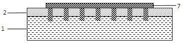
[0030] (1) Using PECVD to grow 100nmSi on the GaN heterojunction material formed by AlGaN barrier layer 2 / GaN channel layer 1 3 N 4 3 and 100nmSiO 2 4 Composite media layer, such as diagram 2-1 Shown

[0031] (2) Apply a layer of AZ7908 photoresist on the sample by spin-off and pre-baking, define the source and drain areas through photolithographic exposure, development and post-baking processes, use electron beam evaporation equipment to evaporate 10nm Ni metal 5, Put the sample into the ac...

Embodiment 1

[0040] Reducing the ohmic contact resistance of GaNHEMT devices based on nano-micropore technology includes the following steps:

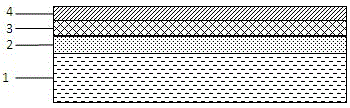
[0041] (1) The channel layer 1 of the GaN heterojunction material with two-dimensional electron gas is made of GaN, AlGaN or InGaN material, and the barrier layer 2 is made of AlGaN, InAlN or AlN material containing Si. 3 N 4 3 and SiO 2 4 Composite dielectric layer; the Si 3 N 4 3 and SiO 2 4The dielectric material can be grown by PECVD, sputtering and thermal evaporation methods, among which Si 3 N 4 3 and SiO 2 4The thickness of the medium is 50nm, Si 3 N 4 3 The etching rate of the material in the buffered hydrofluoric acid solution is higher than that of SiO 2 4 The material should be more than 5 times lower;

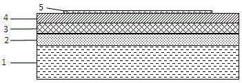
[0042] (2) Use photolithography to define the ohmic area, evaporate a thin layer of Ni metal 5 in the ohmic contact area, and peel off the thin Ni metal 5 in the ohmic area by a metal stripping process; the thickness of the thin Ni metal 5 is ...

Embodiment 2

[0050] Reducing the ohmic contact resistance of GaNHEMT devices based on nano-micropore technology includes the following steps:

[0051] (1) The channel layer 1 of the GaN heterojunction material with two-dimensional electron gas is made of GaN, AlGaN or InGaN material, and the barrier layer 2 is made of AlGaN, InAlN or AlN material containing Si. 3 N 4 3 and SiO 2 4 Composite dielectric layer; the Si 3 N 4 3 and SiO 2 4The dielectric material can be grown by PECVD, sputtering and thermal evaporation methods, among which Si 3 N 4 3 and SiO 2 4 The thickness of the medium is between 50nm and 200nm, Si 3 N 4 3 The etching rate of the material in the buffered hydrofluoric acid solution is higher than that of SiO 2 4 The material should be more than 6 times lower;

[0052] (2) Use photolithography to define the ohmic area, evaporate a thin layer of Ni metal 5 in the ohmic contact area, and peel off the thin Ni metal 5 in the ohmic area by a metal stripping process; the thickness of the ...


PUM

PropertyMeasurementUnit
Thicknessaaaaaaaaaa
Thicknessaaaaaaaaaa
Thicknessaaaaaaaaaa

Abstract

The invention discloses a method of reducing GaN HEMT device ohm contact resistance. The method comprises the following steps of Si3N4 and SiO2 composite dielectric layer growing on a GaN heterojunction material; (2) ohm area thin layer Ni evaporating and stripping; (3) Ni metal nanocluster making and SiO2 dielectric layer etching; (4) photoresist mask layer making; (5) photoresist mask layer etching through oxygen plasma; (6) Si3N4 and SiO2 composite dielectric layer etching; (7) GaN heterojunction micropore making; (8) evaporating / stripping / annealing to form ohm contact. By means of the method, problems of high GaN ohm contact resistivity and a bad metal morphology are solved. The method has the following advantages that (1) the ohm alloy temperature can be lowered; the ohm metal surface and edge morphology can be improved; (2) the micro channel dimension can be controlled through nanodots; the dimension can reach a nanometer level; an electron beam technical preparation way is not required; the technical time consumption is low; (3) and low ohm contact resistance can be acquired.

Description

Technical field [0001] The invention is a method for reducing the ohmic contact resistance of a GaN HEMT (High Electron Mobility Transistor) device on a GaN (Gallium Nitride) material by using nano-micropore technology, and belongs to the technical field of semiconductor device preparation. technical background [0002] GaNHEMT devices have the characteristics of high withstand voltage, high output power density, high temperature resistance, and high operating frequency, and have important application values ​​in communications, radar detection, and power management. The performance of the ohmic contact has a great influence on the performance of the GaNHEMT device. Reducing the ohmic contact of the GaNHEMT device and improving the surface and edge morphology of the ohmic contact are critical to improving the performance of the GaNHEMT device. To this end, a variety of technologies have been developed to improve GaNHEMT ohmic contact, including low-temperature ohmic contact tech...

Claims


Application Information

Patent Timeline
IPC IPC(8): H01L21/336H01L21/28B82Y40/00H01L29/778H01L29/20
CPCH01L21/28H01L29/2003H01L29/66431H01L29/778
Inventor 周建军孔岑郁鑫鑫
Owner NO 55 INST CHINA ELECTRONIC SCI & TECHNOLOGYGROUP CO LTD
Why Eureka
Try Eureka