Back passivation solar cell and preparation method thereof

A solar cell and back electric field technology, applied in circuits, electrical components, photovoltaic power generation, etc., can solve the problems of increased battery series resistance, decreased fill factor, and limited improvement of battery efficiency, achieving increased carrier life, reduced preparation process, The effect of excellent passivation effect

Active Publication Date: 2017-12-08
BYD CO LTD
View PDF4 Cites 4 Cited by
  • Summary
  • Abstract
  • Description
  • Claims
  • Application Information

AI Technical Summary

Problems solved by technology

[0006] The rear passivated crystalline silicon solar cells prepared by the current aluminum oxide passivation process need to deposit two layers of films on the back, namely the aluminum oxide passivation layer and the silicon nitride protective layer. Use laser ablation to form grooves with a certain width and spacing distance, and then print conductive aluminum paste. The aluminum paste forms an aluminum back field through laser etching grooves and silicon wafers, because the area of ​​the groove is small, and the silicon nitride layer has a considerable Therefore, the series resistance of the battery increases, the fill factor decreases, and the efficiency of the battery is limited.

Method used


Image

  • Back passivation solar cell and preparation method thereof
  • Back passivation solar cell and preparation method thereof

Examples


preparation example Construction

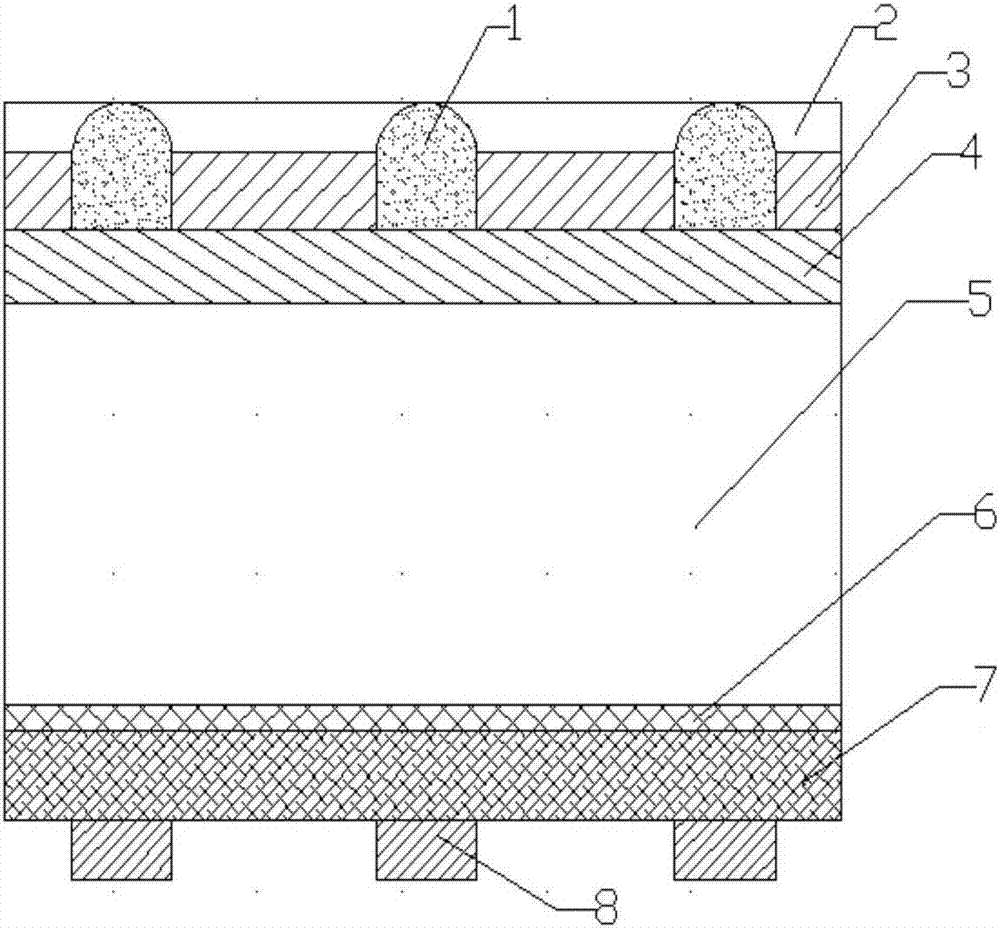
[0028] The present invention also provides a method for preparing a back-passivated solar cell as described above, comprising preparing a front electrode on the light-facing surface of a silicon wafer, and preparing an aluminum layer and a back electrode sequentially on the back-light surface of the silicon wafer; the step of preparing the aluminum layer include:

[0029] S1. Adsorption of alkyl aluminum on silicon wafer;

[0030] S2. The silicon wafer adsorbed with alkylaluminum is contacted with hydrogen, and the passivation aluminum layer is obtained by depositing on the backlight surface of the silicon wafer by atomic layer deposition;

[0031] S3. Depositing a layer of metal aluminum on the passivation aluminum layer to obtain a back electric field aluminum layer.

[0032] Specifically, a method for preparing a back passivated solar cell is characterized in that the step of preparing an aluminum layer comprises:

[0033] S1. Alkyl aluminum is adsorbed on the backlight s...

Embodiment 1

[0067] Step 1: Preparation of anti-reflection coating

[0068] The size of the silicon wafer used is: 156mm×156mm, and the thickness is 200μm. After the silicon wafer is textured, diffused and etched, the backlight surface of the silicon wafer is polished. Then, a silicon nitride anti-reflection film layer with a thickness of 80±4 nm and a refractive index of 2.10±0.03 is prepared by PECVD on the light-facing surface of the silicon wafer.

[0069] Step 2: Preparation of passivated aluminum layer

[0070] A passivation aluminum layer with a certain thickness is deposited by microwave electron cyclotron resonance plasma-assisted atomic layer deposition. A passivated aluminum layer is prepared as a reaction cycle, which is divided into four steps: the first step, that is, trimethylaluminum enters the deposition vacuum chamber under the carrying of high-purity argon, and trimethylaluminum is adsorbed on The backlight surface of the silicon wafer is saturated. In this step, the g...

Embodiment 2

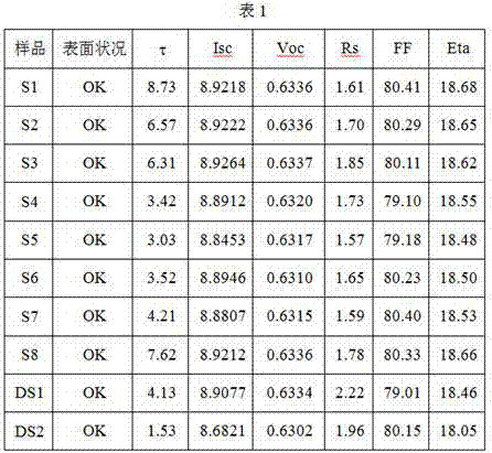
[0082] Change the time for depositing the passivation aluminum layer in step 2 in embodiment 1 to 200s, so that the thickness of the passivation aluminum layer becomes 2-3nm, and the rest are the same as in embodiment 1.

[0083] The solar cell obtained in this example is denoted as S2.


PUM

PropertyMeasurementUnit
thicknessaaaaaaaaaa
thicknessaaaaaaaaaa
thicknessaaaaaaaaaa

Abstract

The invention relates to a solar cell. The solar cell comprises a silicon wafer, a front-surface electrode, an aluminum layer and a back electrode, wherein the front-surface electrode is arranged on a light surface of the silicon wafer, the aluminum layer and the back electrode are arranged on a backlight surface of the silicon wafer, the aluminum layer is arranged on a surface of the backlight surface of the silicon wafer, the back electrode is arranged on a surface of the aluminum layer, and minority carrier lifetime of backlight surface of the silicon wafer in contact with the aluminum layer is 3-10 microseconds. The invention also provides a preparation method of a back passivation solar cell. The solar cell prepared by the method is simple in process and good in passivation effect, the series resistance of the battery is greatly reduced, the filling factor of the battery is obviously increased, and the photoelectric conversion efficiency is also improved; and compared with the solar cell only comprising the aluminum layer on the backlight surface, the short-circuit current and the open-circuit voltage of the battery both can be increased to a great extent, the series resistance is also reduced, and thus, the conversion efficiency of the battery is remarkably improved.

Description

technical field [0001] The invention relates to a back passivated solar cell and a preparation method thereof. Background technique [0002] Existing solar cells generally include a silicon wafer, a front electrode on the light-facing surface, and a back battery and a back electrode on the back-light surface. The positive electrode outputs the negative current of the battery, and the back electric field has a back electrode and a back electric field formed by printing aluminum conductive paste on the back light surface and then sintering on the back light surface. [0003] The aluminum back field can reduce the minority carrier concentration and reduce the recombination, but it still cannot compare with the passivation effect brought by the dielectric layer. UNSW proposed the emitter and rear passivation (PERC) structure and the emitter and rear passivation local diffusion (PERL) structure as early as the 1990s. In the early designs, both structures were passivated with a s...

Claims


Application Information

Patent Timeline
Patent Type & Authority Applications(China)
IPC IPC(8): H01L31/068H01L31/0224H01L31/0216H01L31/18
CPCH01L31/02167H01L31/022425H01L31/068H01L31/1804H01L31/1868Y02E10/547Y02P70/50
Inventor 谭伟华孙玉星孙翔徐华毕
Owner BYD CO LTD
Why Eureka
Try Eureka