White light light-emitting diode device and encapsulation method without gold thread

A LED device, no gold wire technology, applied in semiconductor devices, electrical components, circuits, etc., to achieve the effect of reducing costs, efficient process, and solving heat dissipation problems

Inactive Publication Date: 2013-06-05
KUSN KAIWEI ELECTRONICS
View PDF4 Cites 3 Cited by
  • Summary
  • Abstract
  • Description
  • Claims
  • Application Information

AI Technical Summary

Problems solved by technology

[0003] In order to solve the above-mentioned technical problems, the object of the present invention is to provide a white light LED device and its packaging method without gold wire, which does not need to pass gold wire and phosphor powder coating Covering the process, the process is simple and efficient, which solves the shortcomings caused by the gold wire of the LED device

Method used


Image

  • White light light-emitting diode device and encapsulation method without gold thread
  • White light light-emitting diode device and encapsulation method without gold thread
  • White light light-emitting diode device and encapsulation method without gold thread

Examples


Embodiment 1

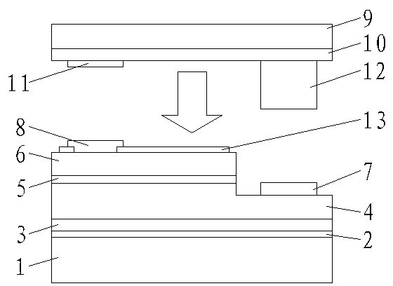
[0027] like figure 1 As shown, a white light LED device of the present invention includes a single crystal fluorescent material composite functional unit and an LED light-emitting chip, and the single crystal fluorescent material composite functional unit is arranged on one side of the LED light-emitting chip; the single crystal fluorescent material composite functional unit includes a single crystal The fluorescent material layer 9 , the transparent conductive layer 10 and the metal electrodes 11 and 12 , the single crystal fluorescent material layer 9 is arranged at one end of the transparent conductive layer 10 , and the metal electrodes 11 and 12 are arranged at the other end of the transparent conductive layer 10 . The LED light-emitting chip is stacked sequentially by the substrate layer 1, the buffer layer 2, the u-GaN layer 3, the n-GaN layer 4, the active region 5 and the p-GaN layer 6, and the n-GaN layer 4 is provided with an n-ohmic contact surface 7. A p-ohmic co...

Embodiment 2

[0039] The rest is the same as that of Embodiment 1, except that the single crystal material functional units are arranged on both sides of the LED light-emitting chip to form an LED device capable of emitting light from both sides.

Embodiment 3

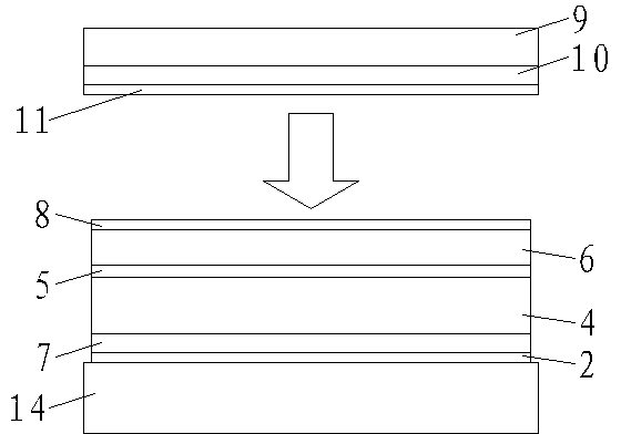
[0041] like image 3 As shown, the rest is the same as that of Embodiment 1, the difference is that it is a LED device with a vertical structure, including a single crystal fluorescent material composite functional unit and an LED light-emitting chip, and the single crystal fluorescent material composite functional unit consists of a single crystal fluorescent material layer 9, The transparent conductive layer 10 and the metal electrode 11 are stacked in sequence, and the LED light-emitting chip consists of a p-ohmic contact surface 8, a p-GaN layer 6, an active region 5, an n-GaN layer 4, an n-ohmic contact surface 7, and a buffer layer 2 Stacked with the base 14 in sequence, the process is simpler and more efficient, and it is helpful to arrange multiple LED light-emitting chips on one base 14, improving the luminous amount and luminous flux of a single LED device.

[0042]The beneficial effects of adopting this technical solution are: encapsulating white light LED devices d...


PUM


Abstract

The invention discloses a white light emitting diode (LED) device which comprises a compound functional unit of monocrystal fluorescent materials and an LED shining chip. The compound functional unit of monocrystal fluorescent materials is arranged on one side of the LED shining chip, and comprises a monocrystal fluorescent material layer, a transparent conducting layer and a metal electrode. The monocrystal fluorescent material layer is arranged at one end of the transparent conducting layer, the metal electrode is arranged at the other end of the transparent conducting layer. Provided is an encapsulation method without gold thread. Technical processes including beating the gold line and fluorescent powder coating are unnecessary. The technical process is simple and efficient. Defects caused by the LED device gold thread are overcome.

Description

technical field [0001] The invention relates to a light emitting semiconductor, in particular to a white light LED device and a gold wire-free packaging method thereof. Background technique [0002] In the prior art, the packaging of LEDs is usually to make PN junction electrodes on the blue light chip, and to make gold wires on the electrodes, which are used to connect the LED chip electrodes to external pins, and then to coat the chips with phosphor. However, the existing technology has the following disadvantages: the manufacture of PN electrodes on the chip affects light output; the process of forming gold wires on the PN electrodes is cumbersome, high in cost, and low in reliability, and the quality of the gold wires directly affects the electrical and optical properties of the chip. Gold is a precious metal, and the gold wire makes the cost of the device high; the contact point between the gold wire and the chip has a large contact resistance, which affects the injecti...

Claims


Application Information

Patent Timeline
Patent Type & Authority Applications(China)
IPC IPC(8): H01L33/48H01L33/50H01L33/00
Inventor 梁月山
Owner KUSN KAIWEI ELECTRONICS
Why Eureka
Try Eureka