Reduced volume interconnect for three-dimensional chip stack

a three-dimensional chip stack and interconnect technology, applied in the field of electric, electronic and computer arts, can solve the problems of limiting the alloys that may be used, increasing the overall package height of the chip stack, and high cost of evaporation or other solder deposition methods, so as to reduce the overall height/size of the interconnect, reduce the height of the stacked package, and reduce the standoff height

Active Publication Date: 2016-07-21
IBM CORP
View PDF5 Cites 3 Cited by
  • Summary
  • Abstract
  • Description
  • Claims
  • Application Information

AI Technical Summary

Benefits of technology

[0009]Techniques of the present invention can provide substantial beneficial technical effects. For example, one or more embodiments may provide reduced standoff height, which reduces the overall height / size of the interconnect and reduces stacked package height, improved power efficiency, increased bandwidth and / or reduced cost.

Problems solved by technology

However, plating, evaporation or other solder deposition methods are typically expensive and complex and limit the alloys that may be used.
Additionally, conventional solder deposition methods produce a spacing between adjacent chips, referred to herein as standoff height, which substantially increases the overall package height of the chip stack and furthermore is not sufficient for high-frequency signals.

Method used


Image

  • Reduced volume interconnect for three-dimensional chip stack
  • Reduced volume interconnect for three-dimensional chip stack
  • Reduced volume interconnect for three-dimensional chip stack

Examples


Embodiment Construction

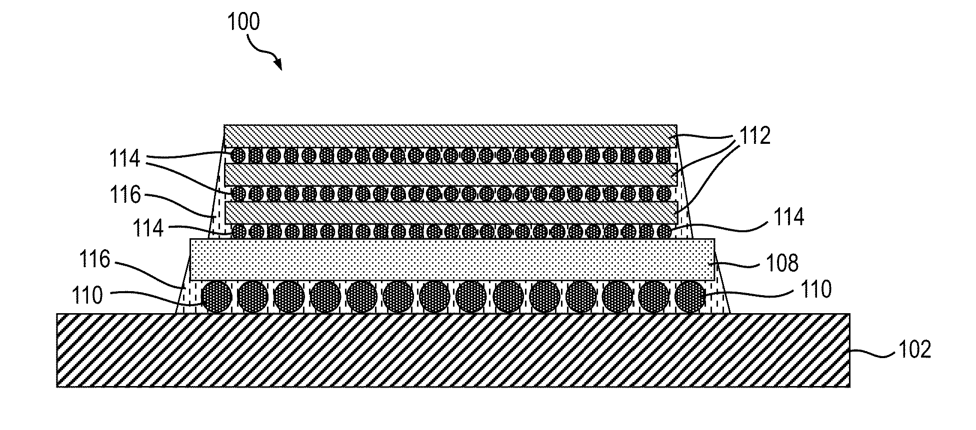
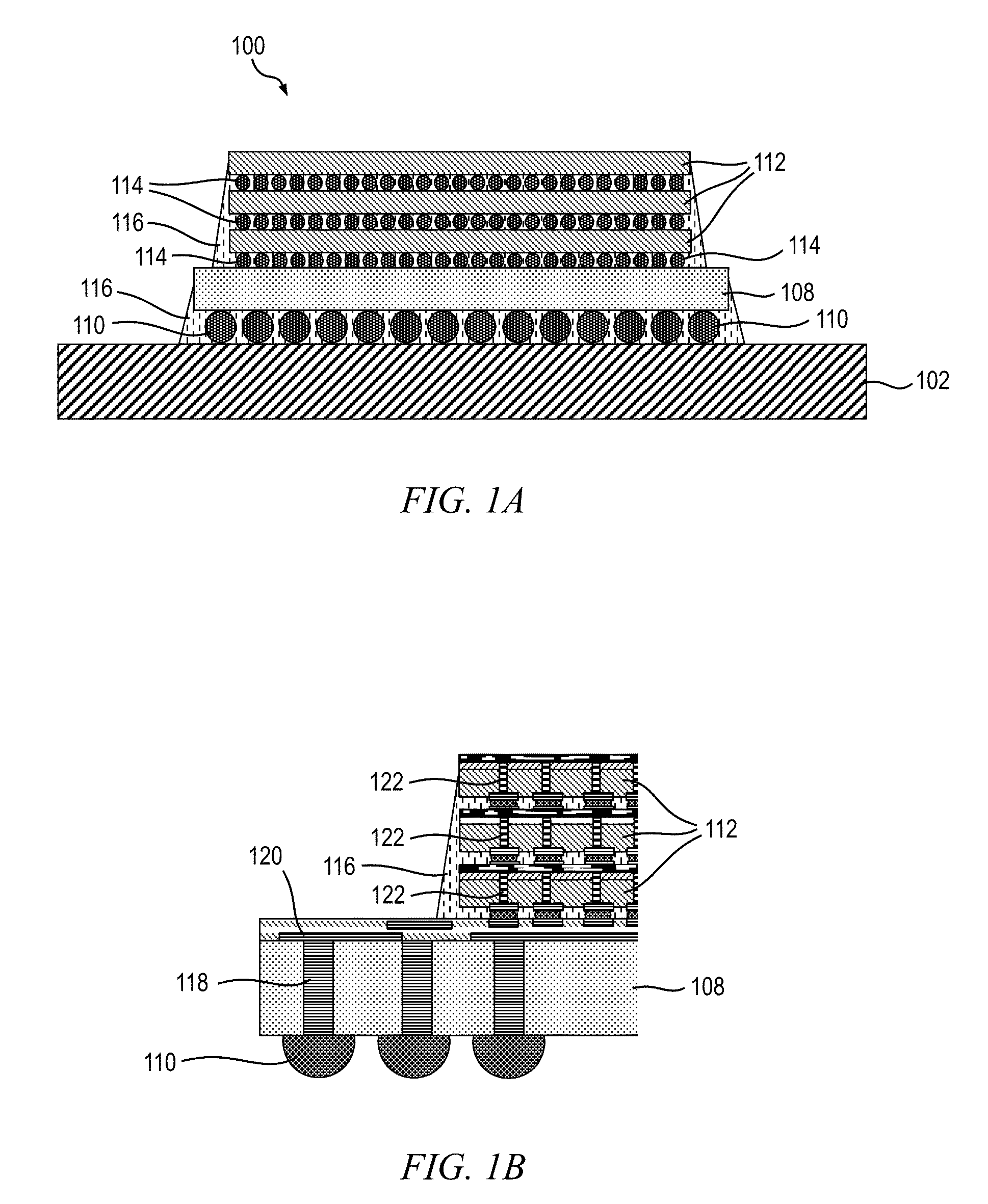
[0019]Embodiments of the present invention will be described herein in the context of illustrative interconnect structures for 3D chip stacks and for methods of making same. It is to be appreciated, however, that the invention is not limited to the specific apparatus and / or methods illustratively shown and described herein. Rather, embodiments of the invention are directed to a reduced volume interconnect for decreasing an interconnect height between adjacent silicon layers of a chip stack. Moreover, it will become apparent to those skilled in the art given the teachings herein that numerous modifications can be made to the embodiments shown that are within the scope of the claimed invention. Thus, no limitations with respect to the embodiments shown and described herein are intended or should be inferred.

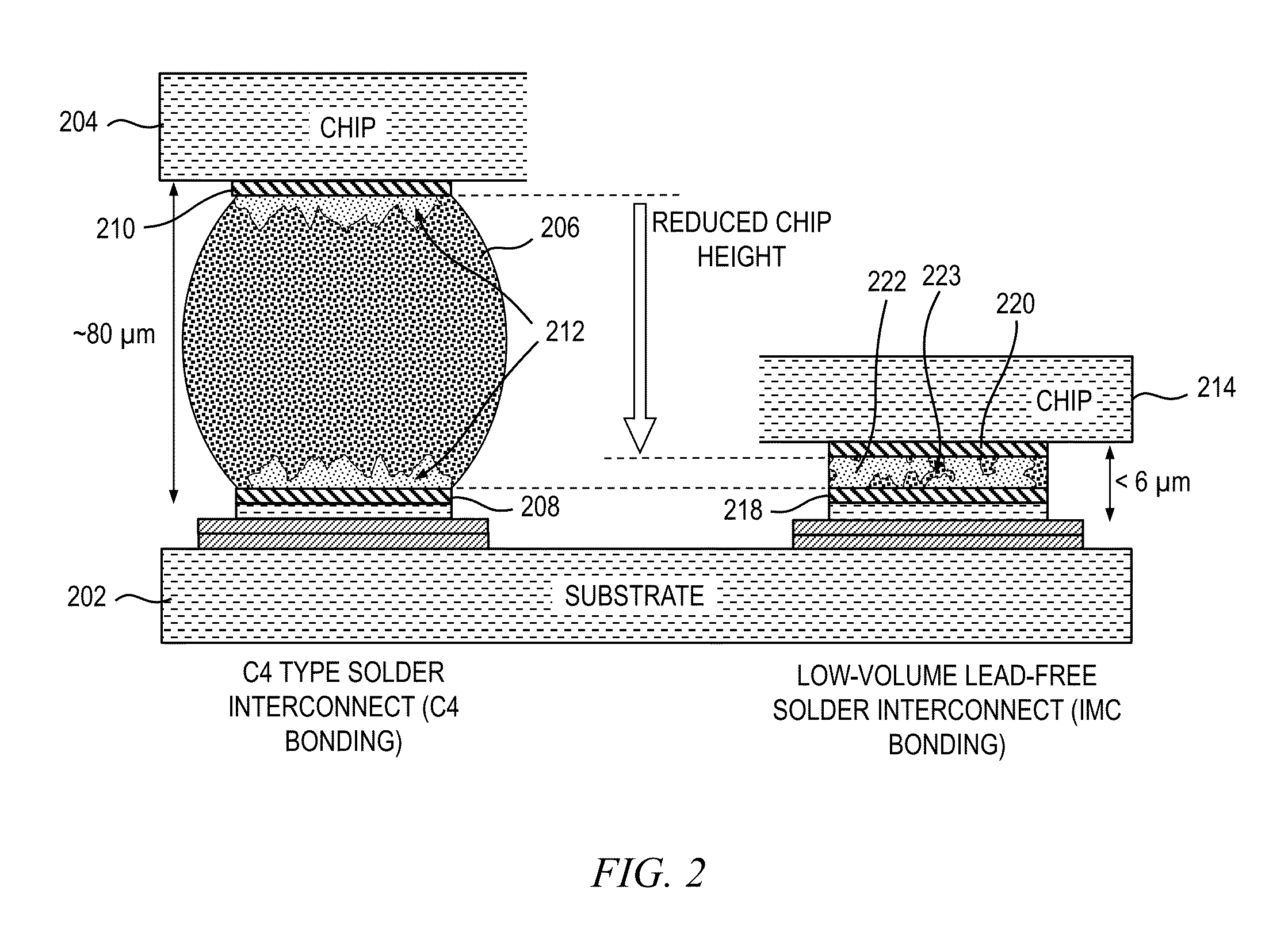
[0020]As previously stated, 3D chip stacking relies on metallized interconnect structures formed between adjacent silicon layers for providing electrical communication therebetween...


PUM


Abstract

A method of forming a reduced volume interconnect for a chip stack including multiple silicon layers, the method including: forming multiple conductive structures, each of at least a subset of the conductive structures having a volume of conductive material for a corresponding under bump metallurgy pad onto which the conductive structure is transferred that is configured such that a ratio of an unreflowed diameter of the conductive structure to a diameter of the corresponding pad is about one third-to-one or less; transferring the conductive structures to the silicon layers; stacking the silicon layers in a substantially vertical dimension such that each of the conductive structures on a given silicon layer is aligned with a corresponding electrical contact location on an underside of an adjacent silicon layer; and heating the interconnect so as to metallurgically bond multiple electrical contact locations of adjacent silicon layers.

Description

BACKGROUND OF THE INVENTION[0001]The present invention relates generally to the electrical, electronic and computer arts, and, more particularly, to integrated circuit (IC) interconnects.[0002]Three-dimensional (3D) chip stacking relies on metallized interconnect structures between silicon layers to enable electrical communication between the respective chips. Chip stacking, as the name suggests, refers to an IC packaging methodology in which a completed computer chip (e.g., dynamic random access memory (DRAM)) is placed on top of another chip (e.g., a central processing unit (CPU)). As a result, two chips that were traditionally centimeters apart on a circuit board are now less than a millimeter apart. This reduces power consumption and also improves bandwidth by a significant amount.[0003]Although several options exist for making 3D interconnect structures, soldering remains one of the most popular. However, plating, evaporation or other solder deposition methods are typically exp...

Claims


Application Information

Patent Timeline
Patent Type & Authority Applications(United States)
IPC IPC(8): H01L25/065H01L21/56H01L23/31H01L25/00H01L23/00
CPCH01L25/0657H01L2224/16012H01L24/06H01L24/17H01L24/81H01L23/3107H01L21/565H01L24/11H01L2225/06513H01L2224/0401H01L2224/8109H01L2224/8112H01L2224/81815H01L2224/8121H01L2224/81201H01L2224/11334H01L2224/811H01L2924/10253H01L2224/16503H01L2224/16145H01L2225/06517H01L25/50H01L24/19H01L2224/81203H01L24/03H01L24/05H01L24/13H01L24/16H01L2224/0381H01L2224/05147H01L2224/05647H01L2224/05655H01L2224/11003H01L2224/1141H01L2224/1144H01L2224/11849H01L2224/13109H01L2224/13111H01L2224/16146H01L2224/16227H01L2224/17181H01L2224/73204H01L2224/81022H01L2224/81065H01L2224/81447H01L2224/81455H01L2224/8181H01L2224/81986H01L2225/06541H01L2924/15311H01L2924/3511H01L2924/381H01L2924/3841H01L2924/00012H01L2924/00014H01L2924/01047H01L2924/01029H01L24/14H01L2224/0612H01L2224/065H01L2224/14104
Inventor GRUBER, PETER A.SAKUMA, KATSUYUKISHIH, DA-YUAN
Owner IBM CORP
Why Eureka
Try Eureka