3D printed active electronic materials and devices

a technology of electronic materials and active materials, applied in the direction of additive manufacturing processes, instruments, applying layer means, etc., can solve the problems of difficult to achieve seamless interweaving of electronics, limited 3d printing to components, plastic parts and metal lines

Active Publication Date: 2016-07-28
THE TRUSTEES FOR PRINCETON UNIV
View PDF1 Cites 39 Cited by
  • Summary
  • Abstract
  • Description
  • Claims
  • Application Information

AI Technical Summary

Benefits of technology

[0008]In producing an active electronic device, the disclosed method may also include dissolving or suspending a printable material in a composition comprising...

Problems solved by technology

However, to date, 3D printing has been limited to components such as plastic parts and metal lines, as well as to specific plastics, passive conductors, and a few biological materials.
Achieving seamless integration of diverse materials with 3D printing is a significant challenge that requires overcoming discrep...

Method used


Image

  • 3D printed active electronic materials and devices
  • 3D printed active electronic materials and devices
  • 3D printed active electronic materials and devices

Examples


Embodiment Construction

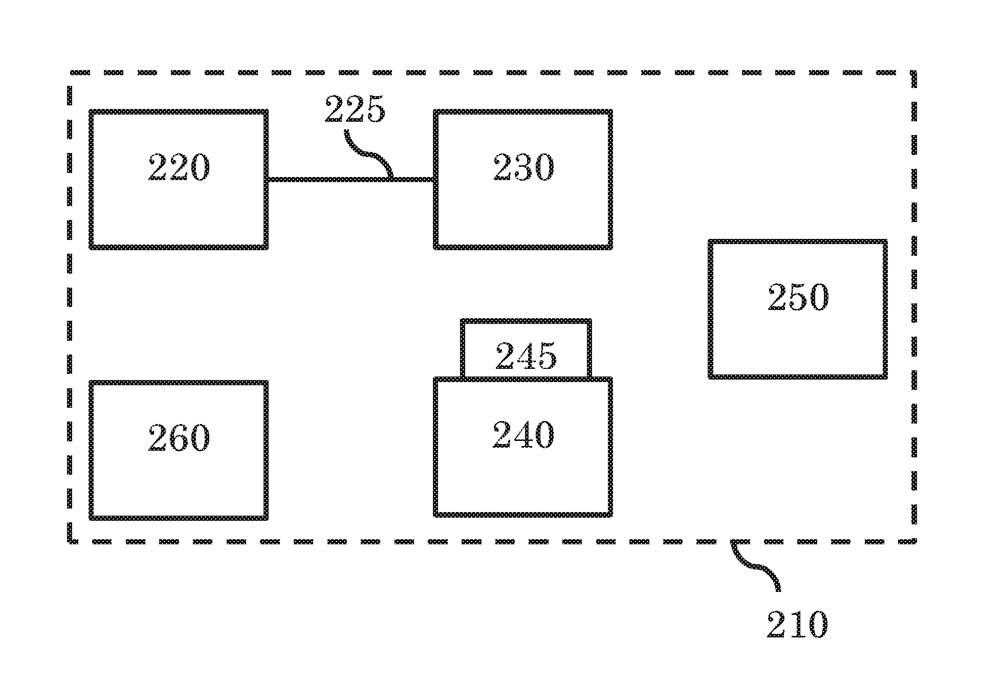
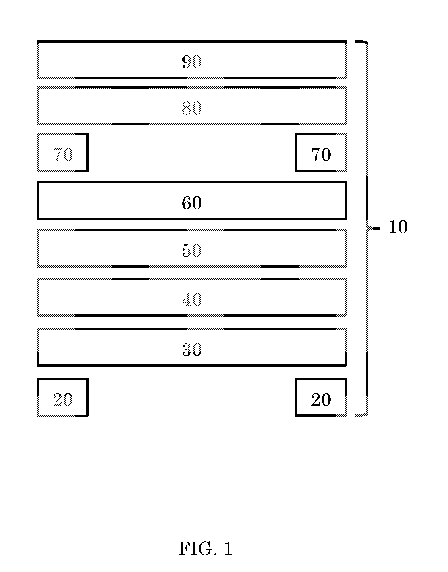
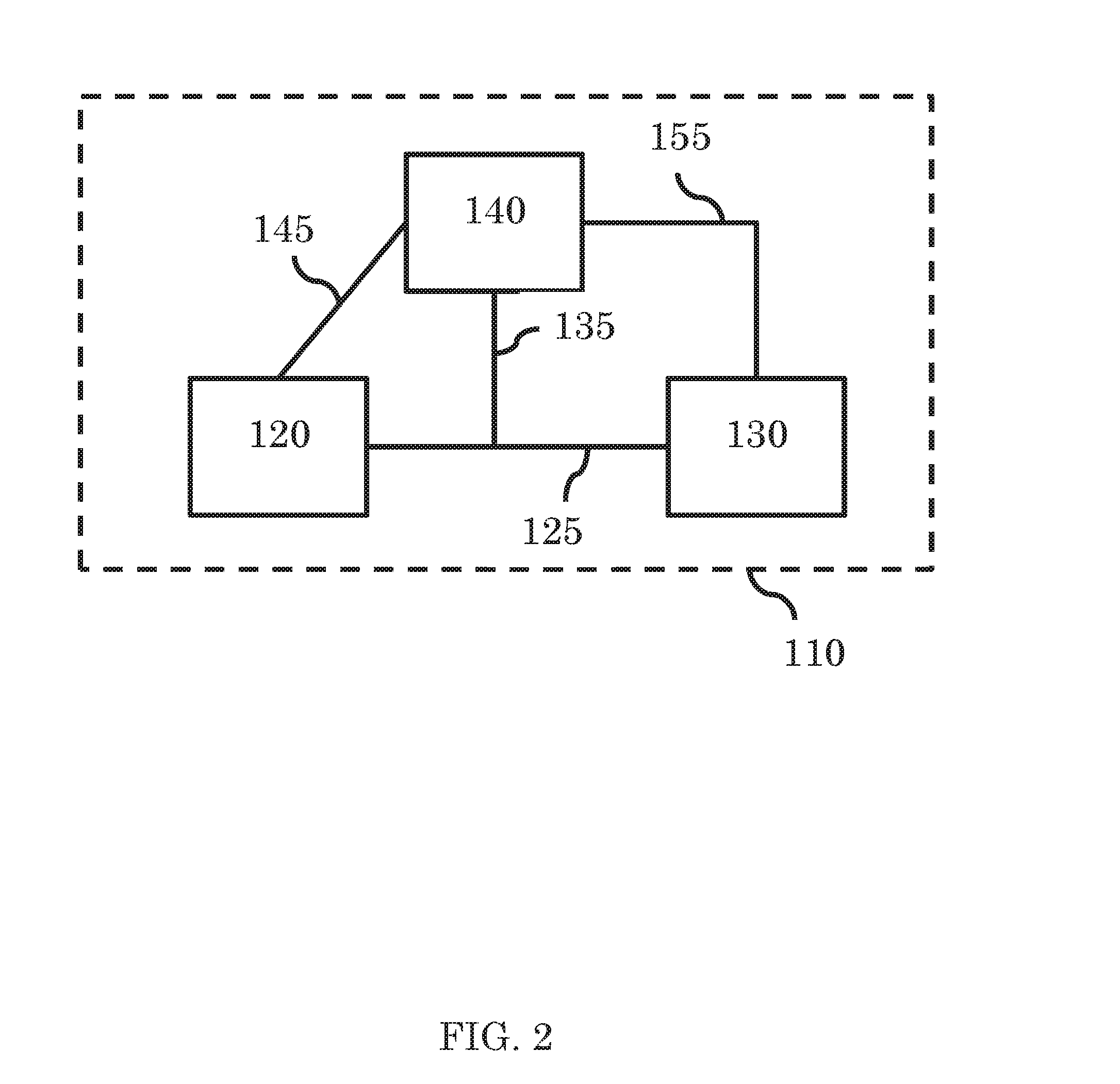
[0014]The novel methods and systems described herein are aimed at enabling the seamless interweaving of electronics in three dimensional devices, generally built from the bottom up.

[0015]The present invention discloses a method of making a device, which comprises 3D printing an active electronic device. These devices generally contain semiconducting materials, which include but are not limited to silicon, silicon-based compounds, germanium, germanium based compounds, cadmium-based compounds, and gallium-based compounds. Those skilled in the art will recognize that this list is non-exhaustive.

[0016]The present invention also may require 3D printing of additional materials or layers beyond a semiconductive material. Those layers may include an elastomeric matrix, organic polymers as charge transport layers, solid or liquid metal leads, nanoparticle semiconductors, and a UV-adhesive transparent substrate layer. Other classes of nanoscale functional building blocks and devices may also ...


PUM

PropertyMeasurementUnit
Sizeaaaaaaaaaa
Electrical conductoraaaaaaaaaa
Metallic bondaaaaaaaaaa

Abstract

Disclosed is a process whereby diverse classes of materials can be 3D printed and fully integrated into device components with active properties. An exemplary embodiment shows the seamless interweaving of five different materials, including (1) emissive semiconducting inorganic nanoparticles, (2) an elastomeric matrix, (3) organic polymers as charge transport layers, (4) solid and liquid metal leads, and (5) a UV-adhesive transparent substrate layer, demonstrating the integrated functionality of these materials. Further disclosed is a device for printing these fully integrated 3D devices.

Description

CROSS-REFERENCE TO RELATED APPLICATIONS[0001]This application claims benefit of U.S. Provisional Application No. 62 / 107,126, filed Jan. 23, 2015, which is hereby incorporated in its entirety by reference.STATEMENT REGARDING FEDERALLY SPONSORED RESEARCH OR DEVELOPMENT[0002]This invention was made with government support under Grant No. FA9550-12-1-0368 awarded by the Air Force Office of Scientific Research (AFOSR) and Grant No. D12AP00245 awarded by the Defense Advanced Research Projects Agency (DARPA). The government has certain rights in the invention.BACKGROUND OF THE INVENTION[0003]Three-dimensional (“3D”) printing is a technique that is starting to gain significant attention and commercial interest. However, to date, 3D printing has been limited to components such as plastic parts and metal lines, as well as to specific plastics, passive conductors, and a few biological materials. A significant advance would be the ability to 3D print functional active electronic materials and d...

Claims


Application Information

Patent Timeline
IPC IPC(8): H01L51/00H01L33/06H01L33/38H01L33/56H01L33/62G02C11/00H01L51/50H01L51/52H01L51/56H01L27/32B29C67/00G02C7/04H01L33/00H01L27/15
CPCH01L51/0004B33Y80/00H01L33/06H01L33/38H01L33/56H01L33/62H01L27/15H01L51/502H01L51/5237H01L51/56H01L27/3202B29C67/0055B29C67/0088G02C7/04G02C11/10H01L2933/005H01L2933/0066H01L2251/5369H01L2933/0016B33Y10/00B33Y30/00B33Y50/02B29K2079/00B29K2105/0073B29K2025/06B29K2081/00B29K2083/00B29K2995/0005H01L33/0083Y02E10/549H01L33/005B29C64/106B29C64/209H10K71/13H10K71/191H10K85/1135H10K85/631H10K50/115H10K71/00
Inventor MCALPINE, MICHAEL C.KONG, YONG LIN
Owner THE TRUSTEES FOR PRINCETON UNIV
Why Eureka
Try Eureka