Organic el device and electronic apparatus

a technology of electronic equipment and organic el, which is applied in the direction of organic semiconductor devices, semiconductor devices, diodes, etc., can solve the problems of affecting the reliability of electronic equipment, affecting the protection of organic el devices, and protruding of the filter, etc., and achieves the effect of high reliability of electronic equipmen

Active Publication Date: 2016-08-04
SEIKO EPSON CORP
View PDF4 Cites 9 Cited by
  • Summary
  • Abstract
  • Description
  • Claims
  • Application Information

AI Technical Summary

Benefits of technology

[0026]According to the application example, since the organic EL device is

Problems solved by technology

However, in a case where a plurality of organic EL devices is formed at the same time on a large substrate (motherboard), when formed so that the end portions of the element substrate and the counter substrate have substantially the same position, a problem arises of the filler protruding to the neighboring organic EL device side.
Meanwhile, when formed so that the end portion

Method used


Image

  • Organic el device and electronic apparatus
  • Organic el device and electronic apparatus
  • Organic el device and electronic apparatus

Examples


first embodiment

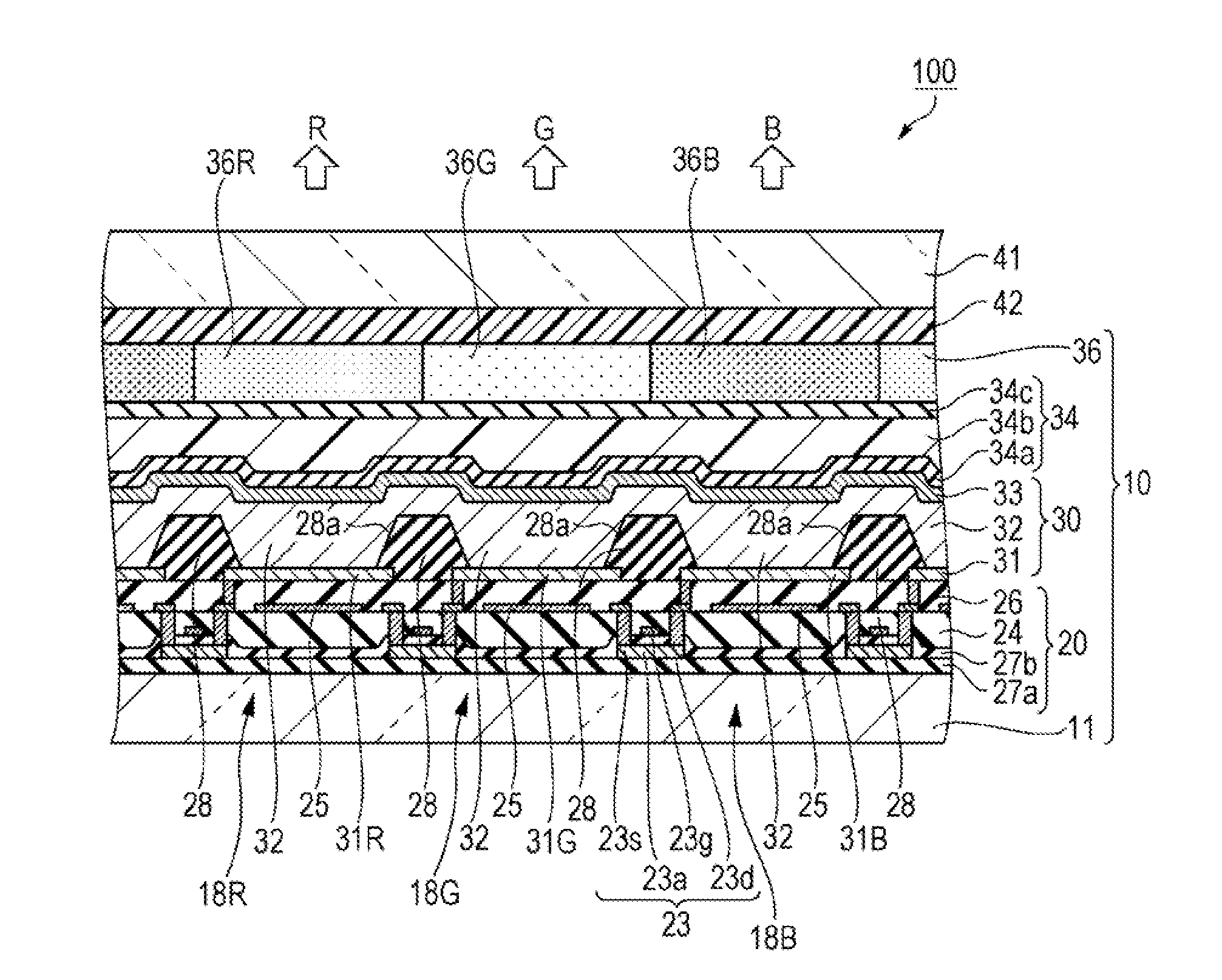
[0042]Organic EL Device

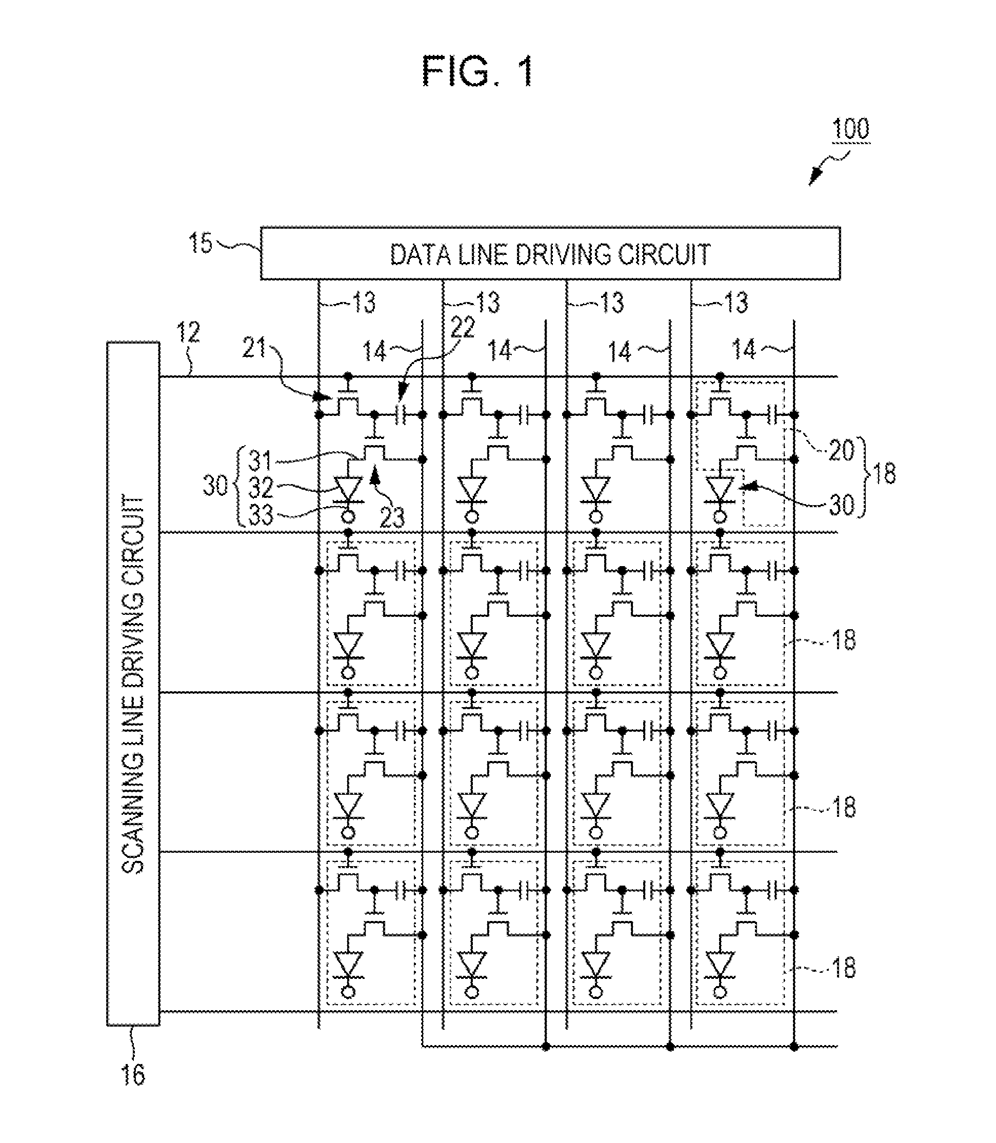
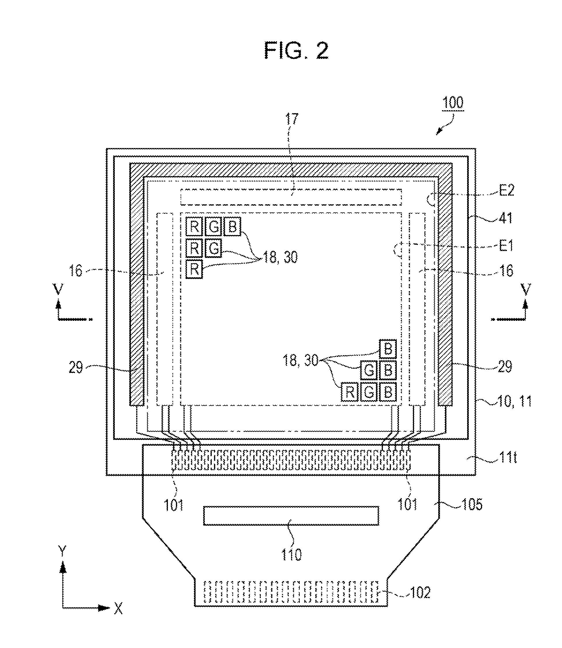
[0043]First, the organic electroluminescence (EL) device of the embodiment will be described with reference to FIGS. 1 to 3. FIG. 1 is an equivalent circuit diagram showing an electrical configuration of the organic EL device of the first embodiment; FIG. 2 is a schematic plan view showing the configuration of the organic EL device of the first embodiment; and FIG. 3 is a schematic plan view showing a pixel arrangement in the first embodiment.

[0044]As shown in FIG. 1, the organic EL device 100 of the embodiment includes plurality of scanning lines 12 and a plurality of data lines 13 that intersect one another, and a plurality of power lines 14 arranged in a line for each of the plurality of data lines 13. The organic EL device includes a scanning line driving circuit 16 to which the plurality of scanning lines 12 is connected, and a data line driving circuit 15 to which the plurality of data lines 13 is connected. A plurality of sub-pixels 18 that is arranged ...

second embodiment

[0136]Organic EL Device

[0137]Next, the organic EL device of the second embodiment will be described with reference to FIG. 9. FIG. 9 is a schematic cross-sectional view showing a structure of the organic EL device of the second embodiment.

[0138]Compared to the organic EL device 100 of the above-described first embodiment, the organic EL device 111 of the second embodiment differs in the shape of the counter substrate 141 and the other parts are substantially the same. Therefore, in the second embodiment, the parts different to the first embodiment will be described in detail, and the other overlapping parts will not be described, as appropriate.

[0139]As shown in FIG. 9, a taper 141a of the organic EL device 111 of the second embodiment is formed on the outer peripheral edge of the filler 42 side on the counter substrate 141. Specifically, the region in which the taper 141a is formed is preferably formed at a position (further to the outside than the second sealing layer 34b in plan ...

third embodiment

[0148]Organic EL Device

[0149]Next, the organic EL device of the third embodiment will be described with reference to FIG. 10. FIG. 10 is a schematic cross-sectional view showing a structure of the organic EL device of the third embodiment.

[0150]Compared to the organic EL device 100 of the above-described first embodiment, the organic EL device 112 of the third embodiment differs in the parts having the projection 36a between the end portion 11a of the base material 11 and the end portion 42a of the filler 42 in plan view, and the other parts are substantially the same. Therefore, in the third embodiment, the parts different to the first embodiment will be described in detail, and the other overlapping parts will not be described, as appropriate.

[0151]As shown in FIG. 10, the counter substrate 41 of the organic EL device 112 of the third embodiment is arranged so as to cover the second sealing layer 34b in plan view, as described above. Further, a projection 36a that is a characteris...


PUM


Abstract

An organic EL device includes an element substrate above which an organic EL element is provided; a counter substrate arranged so as to face the element substrate; a sealing layer arranged between the organic EL element and the counter substrate, and having at least a first sealing layer made from an inorganic material, a planarized second sealing layer, and a third sealing layer formed from an inorganic material; and a filler arranged between the sealing layer and the counter substrate, in which the counter substrate is arranged in a region spaced by a predetermined gap from any end portion of the element substrate, the filler is arranged so as to protrude to the gap from between the element substrate and the counter substrate, and the end portion of the second sealing layer is covered by the filler.

Description

BACKGROUND[0001]1. Technical Field[0002]The present invention relates to an organic EL device and an electronic apparatus.[0003]2. Related Art[0004]The organic electroluminescence (EL) device has a structure in which a light emitting layer formed from a light emitting material is interposed between an anode (pixel electrode) and a cathode (counter electrode). The organic EL devices are adhered to an element substrate and a counter substrate via a sealing material and a filler. A connection terminal that electrically connects the organic EL device and an external apparatus is provided on the element substrate.[0005]JP-A-2014-89803 discloses an organic EL device with a structure in which an end portion of the element substrate and an end portion of the counter substrate are arranged at approximately the same position in plan view, except for a region in which the connection terminal is arranged.[0006]However, in a case where a plurality of organic EL devices is formed at the same time...

Claims


Application Information

Patent Timeline
IPC IPC(8): H01L51/52H01L27/32
CPCH01L51/5246H01L2251/558H01L27/322H10K59/38H10K50/841H10K50/8426H10K50/844
Inventor AKAGAWA, SUGURUKOSHIHARA, TAKESHI
Owner SEIKO EPSON CORP
Why Eureka
Try Eureka