Charge trapping nonvolatile memory devices, methods of fabricating the same, and methods of operating the same

Active Publication Date: 2016-08-18
SK HYNIX INC
View PDF10 Cites 15 Cited by
  • Summary
  • Abstract
  • Description
  • Claims
  • Application Information

AI Technical Summary

Benefits of technology

[0014]According to another embodiment, there is provided a method of operating a charge trapping nonvolatile memory device including a plurality of word lines including first, second, and third word lines and arranged along rows, a plurality of bit lines respectively disposed along a plurality of columns, a plurality of source lines extending in parallel to the rows, and a plurality of unit cells respectively located at cross points of the rows and the columns, wherein the plurality of unit cells include a first unit cell located at a Nth row and a Pth column, a second unit cell located at the (N−1)th row and the Pth column, and a third unit cell located at the (N+1)th row and the Pth column, wherein each of N and P is an integer, wherein each of the first, the second, and the third unit cells includes a first charge storage transistor, a selection transistor, and a second charge storage transistor which are connected in series along a column direction, wherein the first charge storage transistor has a first control gate terminal and a source terminal, wherein the selection transistor has a selection gate terminal, wherein the second charge storage transistor has a second control gate terminal and a drain terminal, wherein the source terminal of the first unit cell is electrically connected to the source terminal of the second unit cell, wherein the first control gate terminal, the selection gate terminal, and the second control gate terminal of the first unit cell

Problems solved by technology

In contrast, nonvolatile memory devices retain their stored data when their power supplies are interrupted but tend to operate at lower speeds.
Thus, it may be inconvenient to use MROM devices, PROM devices, and EPROM devices in

Method used


Image

  • Charge trapping nonvolatile memory devices, methods of fabricating the same, and methods of operating the same
  • Charge trapping nonvolatile memory devices, methods of fabricating the same, and methods of operating the same
  • Charge trapping nonvolatile memory devices, methods of fabricating the same, and methods of operating the same

Examples


Embodiment Construction

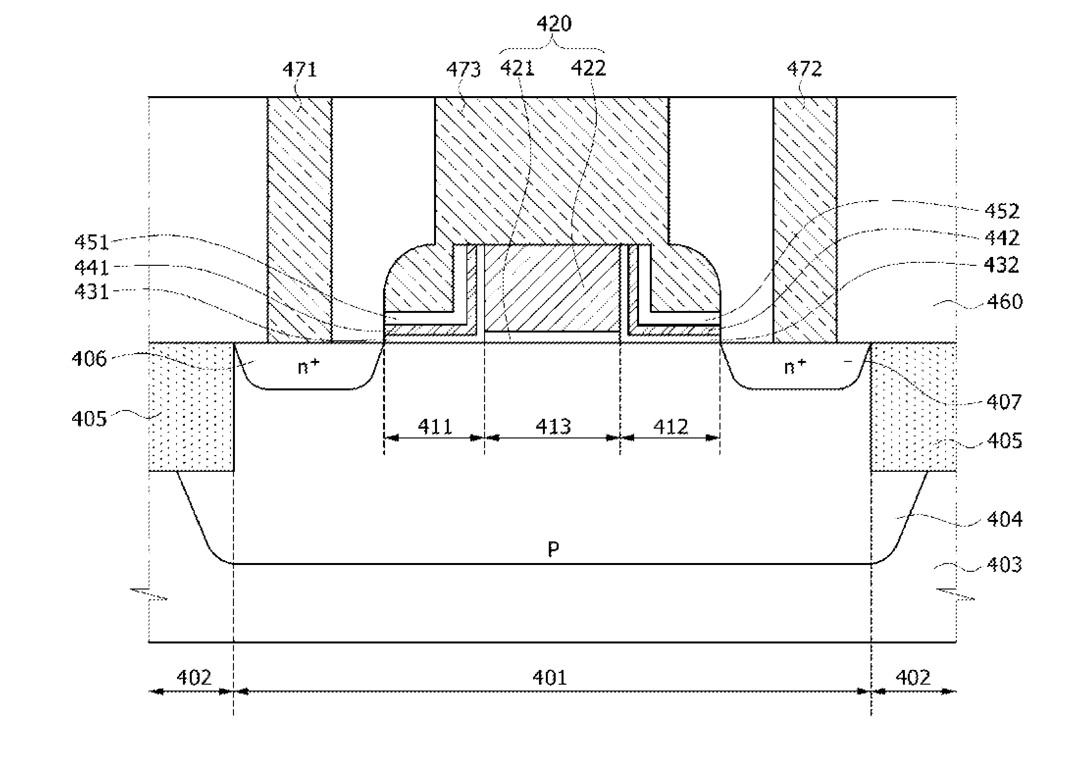
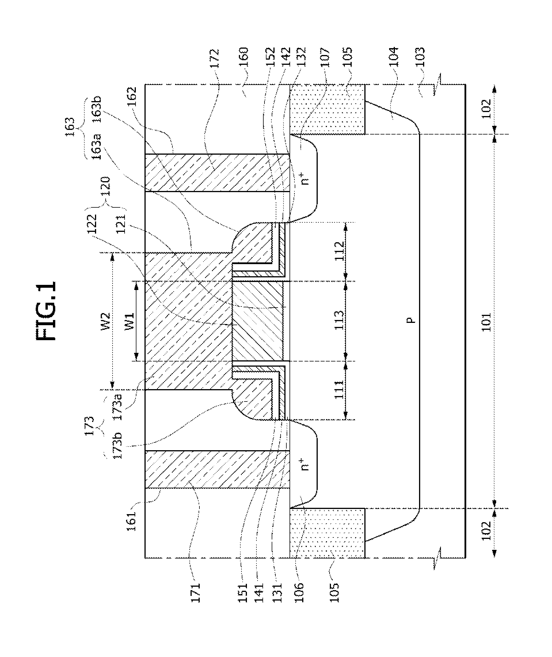
[0035]It will be understood that although the terms first, second, third etc. may be used herein to describe various elements, these elements should not be limited by these terms. These terms are only used to distinguish one element from another element. Thus, a first element in some embodiments could be termed a second element in other embodiments without departing from the teachings of the present disclosure.

[0036]It will also be understood that when an element is referred to as being located “on”“over”, “above”, “under”, “beneath” or “below” another element, it may directly contact the other element, or at least one intervening element may be present therebetween. Accordingly, the terms such as “on”, “over”, “above”, “under”, “beneath”, “below” and the like that are used herein are for the purpose of describing particular embodiments only and are not intended to limit the scope of the present disclosure.

[0037]It will be further understood that when an element is referred to as be...


PUM


Abstract

A charge trapping nonvolatile memory device includes a source region and a drain region disposed in an upper portion of a substrate and spaced apart from each other by a first trapping region, a channel region, and a second trapping region. A gate stack structure is disposed over the channel region. A first stack including a tunnel insulation layer, a first charge trap layer, and a first blocking insulation layer are disposed over the first trapping region. A second stack including a tunnel insulation layer, a second charge trap layer, and a second blocking insulation layer are disposed over the second trapping region. An interlayer insulation layer is disposed over the substrate and covers the gate stack structure. A first contact plug and a second contact plug penetrate the interlayer insulation layer and respectively contact the source region and the drain region. A third contact plug penetrates the interlayer insulation layer, contacts the gate stack structure, and overlaps with the first and the second charge trap layers.

Description

CROSS-REFERENCE TO RELATED APPLICATION[0001]The present application claims priority under 35 U.S.C 119(a) to Korean Application No. 10-2015-0024489 filed on Feb. 17, 2015, which is herein incorporated by reference in its entirety.BACKGROUND[0002]1. Technical Field[0003]Various embodiments of the present disclosure relate to nonvolatile memory devices. More particularly to charge trapping nonvolatile memory devices, methods of fabricating the same, and methods of operating the same.[0004]2. Related Art[0005]Semiconductor memory devices are typically categorized as either volatile memory devices or nonvolatile memory devices. Volatile memory devices lose their stored data when their power supplies are interrupted but have relatively high operating speeds. That is, they read out data stored in memory cells or write data into the memory cells relatively quickly. In contrast, nonvolatile memory devices retain their stored data when their power supplies are interrupted but tend to operate...

Claims


Application Information

Patent Timeline
IPC IPC(8): H01L27/115H01L29/792
CPCH01L29/7923H01L27/1157G11C16/14H10B43/00H10B43/35H01L29/42344H01L29/42348H01L29/40117
Inventor KWON, YOUNG JOON
Owner SK HYNIX INC
Why Eureka
Try Eureka