THROUGH-SILICON VIA (TSV) CRACK SENSORS FOR DETECTING TSV CRACKS IN THREE-DIMENSIONAL (3D) INTEGRATED CIRCUITS (ICs) (3DICs), AND RELATED METHODS AND SYSTEMS

a technology of three-dimensional (3d) integrated circuits and crack sensors, which is applied in the direction of basic electric elements, semiconductor/solid-state device testing/measurement, instruments, etc., can solve problems such as rendering 3d defects, and achieve the effect of increasing the resistance of the doped ring and facilitating direct detection

Active Publication Date: 2016-09-08
QUALCOMM INC
View PDF11 Cites 22 Cited by
  • Summary
  • Abstract
  • Description
  • Claims
  • Application Information

AI Technical Summary

Benefits of technology

[0011]Aspects disclosed in the detailed description include through-silicon via (TSV) crack sensors for detecting TSV cracks in three-dimensional (3D) integrated circuits (ICs) (3DICs). Related methods and systems are also disclosed. To detect cracks in TSVs in a 3DIC that may cause silicon substrate cracks in the 3DIC due to a coefficient of thermal expansion (CTE) mismatch between materials used to create the TSVs and the corresponding substrate, TSV crack sensors are provided in the 3DIC. The TSV crack sensors are disposed around a corresponding TSV in the 3DIC. In one aspect, the TSV crack sensor is comprised of a doped ring disposed around a corresponding TSV. Specifically, a crack that traverses the doped ring will create a discont

Problems solved by technology

If the resistance exceeds a predetermined threshold, a crack may be present in the surrounding silicon substrate, possibly rendering the 3DIC defective.
However, test

Method used


Image

  • THROUGH-SILICON VIA (TSV) CRACK SENSORS FOR DETECTING TSV CRACKS IN THREE-DIMENSIONAL (3D) INTEGRATED CIRCUITS (ICs) (3DICs), AND RELATED METHODS AND SYSTEMS
  • THROUGH-SILICON VIA (TSV) CRACK SENSORS FOR DETECTING TSV CRACKS IN THREE-DIMENSIONAL (3D) INTEGRATED CIRCUITS (ICs) (3DICs), AND RELATED METHODS AND SYSTEMS
  • THROUGH-SILICON VIA (TSV) CRACK SENSORS FOR DETECTING TSV CRACKS IN THREE-DIMENSIONAL (3D) INTEGRATED CIRCUITS (ICs) (3DICs), AND RELATED METHODS AND SYSTEMS

Examples


Embodiment Construction

[0030]With reference now to the drawing figures, several exemplary aspects of the present disclosure are described. The word “exemplary” is used herein to mean “serving as an example, instance, or illustration.” Any aspect described herein as “exemplary” is not necessarily to be construed as preferred or advantageous over other aspects.

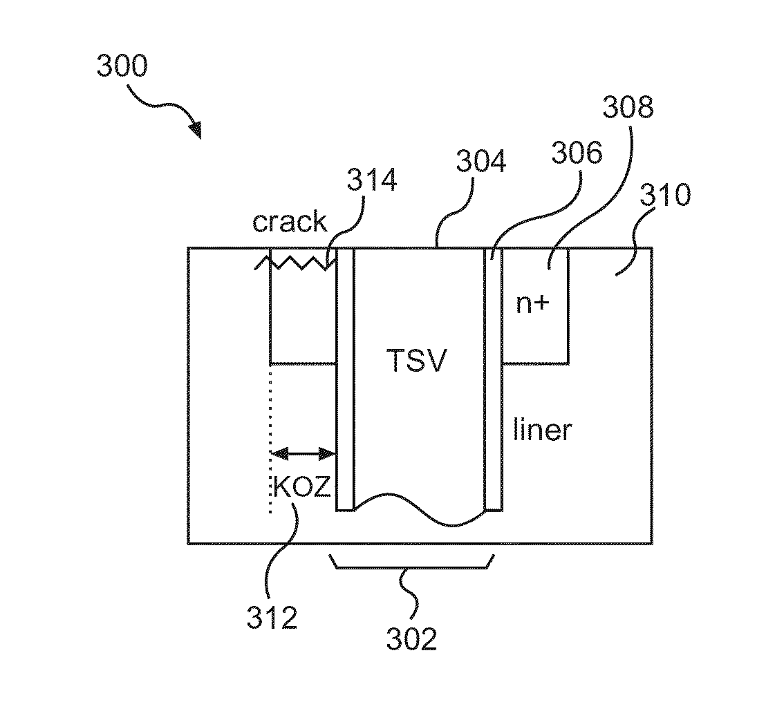
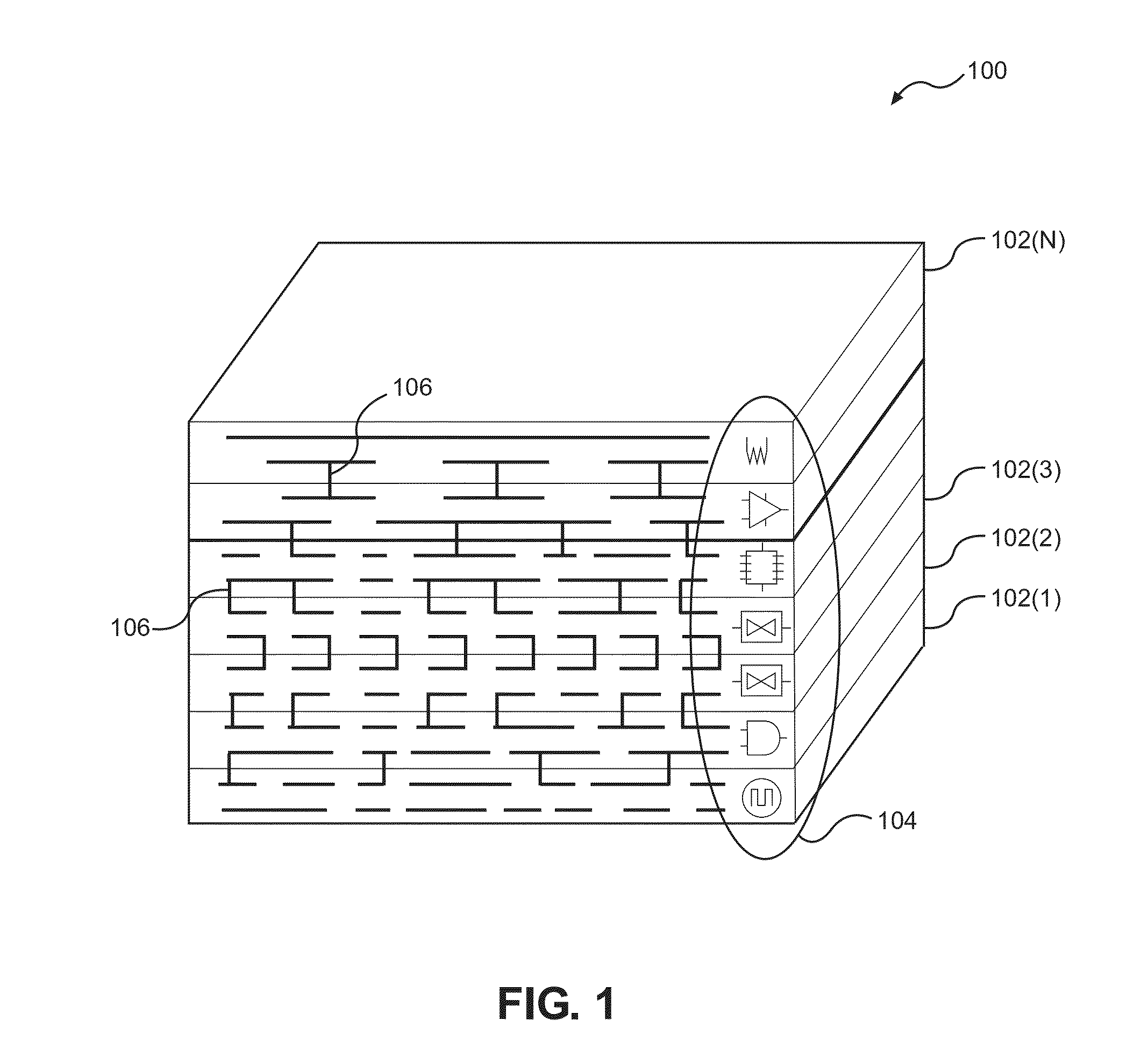
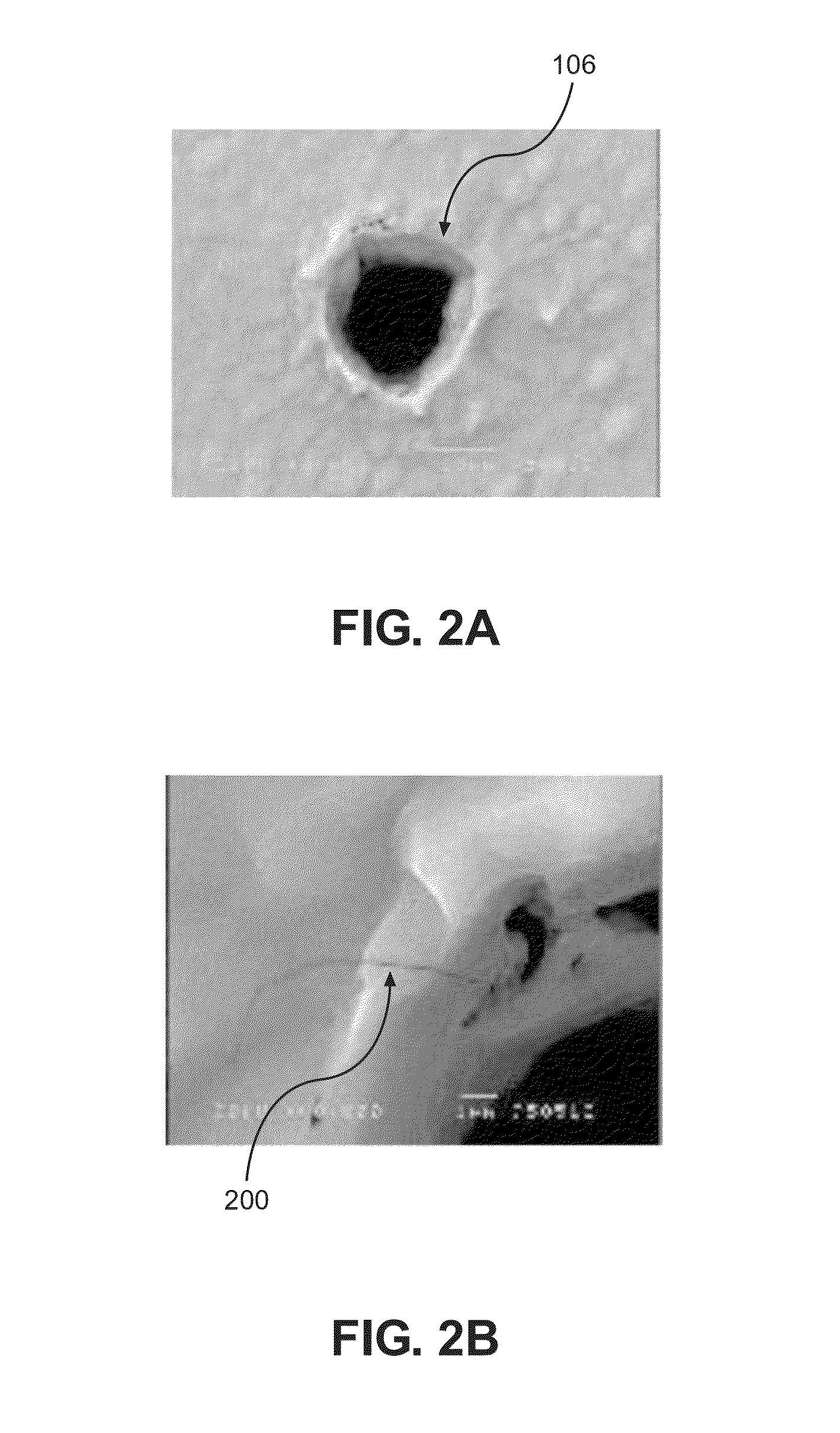
[0031]Aspects disclosed in the detailed description include through-silicon via (TSV) crack sensors for detecting TSV cracks in three-dimensional (3D) integrated circuits (ICs) (3DICs). Related methods and systems are also disclosed. To detect cracks in TSVs in a 3DIC that may cause silicon substrate cracks in the 3DIC due to a coefficient of thermal expansion (CTE) mismatch between materials used to create the TSVs and the corresponding substrate, TSV crack sensors are provided in the 3DIC. The TSV crack sensors are disposed around a corresponding TSV in the 3DIC. In one aspect, the TSV crack sensor is comprised of a doped ring disposed around a corr...


PUM


Abstract

Through-silicon via (TSV) crack sensors for detecting TSV cracks in three-dimensional (3D) integrated circuits (ICs) (3DICs), and related methods and systems are disclosed. In one aspect, a TSV crack sensor circuit is provided in which doped rings for a plurality of TSVs are interconnected in parallel such that all interconnected TSV doped rings may be tested at the same time by providing a single current into the contacts of the interconnected doped rings. In another aspect, a TSV crack sensor circuit is provided including one or more redundant TSVs. Each doped ring for a corresponding TSV is tested independently, and a defective TSV may be replaced with a spare TSV whose doped ring is not detected to be cracked. This circuit allows for correction of a compromised 3DIC by replacing possibly compromised TSVs with spare TSVs.

Description

BACKGROUND[0001]I. Field of the Disclosure[0002]The technology of the disclosure relates generally to through-silicon vias (TSVs) for three-dimensional (3D) integrated circuits (ICs) (3DICs), and more particularly to the detection of silicon substrate surface cracks therein.[0003]II. Background[0004]Computing devices have become commonplace throughout society. The increasing presence of such computing devices has accelerated in part because of the increasing functionality and versatility of such computing devices. This increase in functionality and versatility has been enabled by providing increasingly powerful processing capabilities in small packages as loosely recognized by Moore's Law. As a result, companies have been trying to increase functional integration more quickly than Moore's Law or circuit performance requirements. However, pressures to increase processing capabilities while decreasing the size of integrated circuits (ICs) have strained conventional manufacturing proce...

Claims


Application Information

Patent Timeline
IPC IPC(8): G01R31/28H01L27/06G01R19/165H01L23/58H01L23/64H01L21/66H01L23/48
CPCG01R31/2851H01L22/14H01L22/34G01R19/16533H01L23/481H01L23/585H01L23/647H01L27/0688G01R31/2853G01R31/318513
Inventor LIM, SUNG KYURADOJCIC, RATIBORDU, YANG
Owner QUALCOMM INC
Why Eureka
Try Eureka