Universal I/O Signal Interposer System
- Summary
- Abstract
- Description
- Claims
- Application Information
AI Technical Summary
Benefits of technology
Problems solved by technology
Method used
Image
Examples
second embodiment
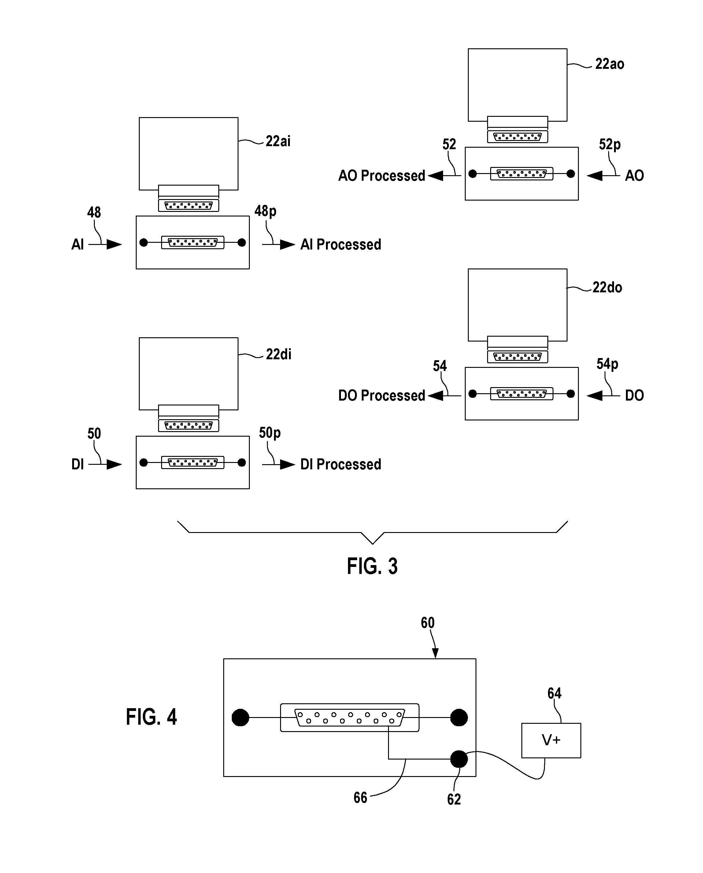
[0053]FIG. 4 illustrates a second embodiment base assembly 60 that is similar to the base assembly 20 but can supply power to the I / O device 12. The base interposer circuit segment of the base assembly 60 includes a power supply terminal 62 that is shown connected to a voltage source 64. The voltage source in the illustrated embodiment is a 24 volt DC voltage source. The base assembly PCB provides electrical circuit communication 66 between the power terminal 62 and the connector half 26b. As shown in FIG. 5, the circuit carrier for use with the base assembly 60 includes a jumper 68 whose ends are connected to the connector half 24a. When the circuit carrier 22 is connected to the base assembly 60 the electrical connector 24 places the jumper 68 in series with the base circuit sections 66, 33. Power is supplied from the voltage source 64 to the I / O device 12 through the line 16.
[0054]An interposer circuit carrier 22 is also a power circuit carrier if the carrier is configured to sup...
third embodiment
[0057]FIG. 6 illustrates a third embodiment base assembly 72 similar to the base assembly 60. The signal interconnection circuit of the base assembly 72 includes a second device-side terminal 74 that is connected to the electrical connector half 24b by electrical circuit communication 76. The interposer circuit carrier 22 used with the base assembly 72 interconnects the power supply terminal 62 with the terminal 74. A power line is connected to the terminal 74 and to the I / O device 12 to supply power to the I / O device through a power line 78 separate from the I / O device signal line 16.
[0058]FIG. 6 illustrates that a signal interconnection circuit may include a plural number of terminals for connections with an I / O device 12. Additional terminals could be provided, for example, to terminate shield conductors extending from the I / O device.
fourth embodiment
[0059]FIG. 7 illustrates a fourth embodiment base assembly 80 similar to the base assembly 72. The signal interconnection circuit of the base assembly 80 includes a second power supply terminal 82 in addition to the power supply terminal 62. Power supply terminal 82 is shown connected to a second voltage source 84 that supplies a different voltage than does the voltage source 64. When an interposer circuit carrier 22 configured to interconnect the power supply terminal 62 to the device power terminal 74 is used, power can be transmitted from the voltage source 54 to the I / O device 12 through the power line 78 as was shown in FIG. 6. When an interposer circuit carrier 22 configured to interconnect the power supply terminal 82 to the device terminal 30 is used, power can be transmitted from the voltage source 84 to the I / O device 12 through the I / O device signal line 16 as was shown in FIG. 4.
PUM
 Abstract
Description
Claims
Application Information


