Through electrode substrate and semiconductor device using through electrode substrate

a technology of through electrode substrate and semiconductor device, which is applied in the direction of resist details, non-metallic protective coating application, printed circuit aspects, etc., can solve the problems of gap generation and defects such as dropout of filler

Active Publication Date: 2016-09-22
DAI NIPPON PRINTING CO LTD
View PDF9 Cites 11 Cited by
  • Summary
  • Abstract
  • Description
  • Claims
  • Application Information

AI Technical Summary

Benefits of technology

[0013]The gas discharge member may include an aperture having an area incre

Problems solved by technology

However, even when attempting to prevent dropout of the filler by such a technique, a gap is generated between the filler and the side wall of the through-hole and a gas reservoir may be generated.
When heat is applied to the

Method used


Image

  • Through electrode substrate and semiconductor device using through electrode substrate
  • Through electrode substrate and semiconductor device using through electrode substrate
  • Through electrode substrate and semiconductor device using through electrode substrate

Examples


first embodiment

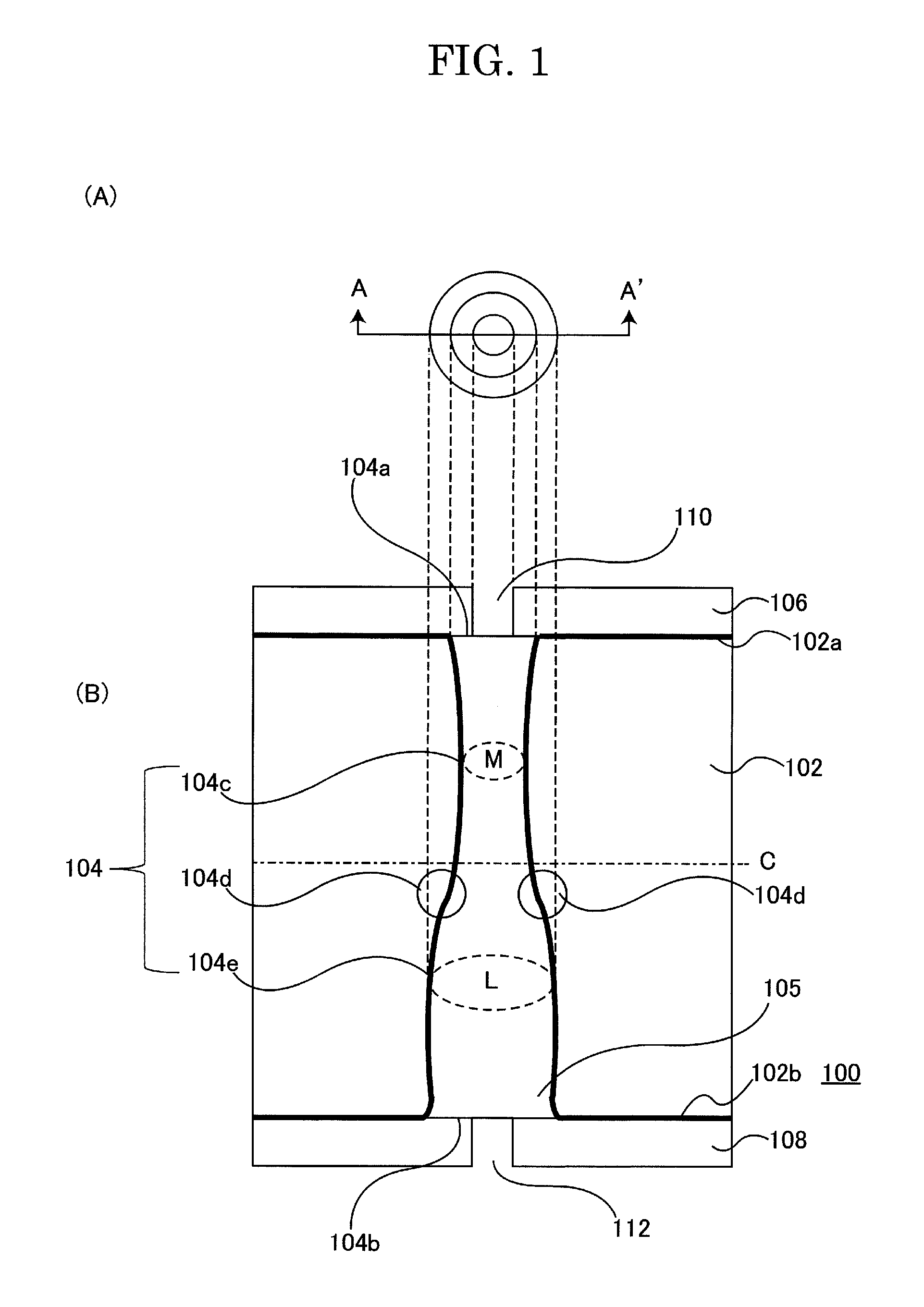
[0043]The structure of a through-hole electrode substrate 100 of the embodiment of the invention related to the present embodiment is explained while referring to FIG. 1. FIG. 1 (A) is a planar diagram of the through-hole electrode substrate 100 of the embodiment of the invention related to the present embodiment seen from the upper surface. FIG. 1 (B) is a cross-sectional diagram of the line A˜A′ in FIG. 1 (A). Both FIGS. 1 (A) and (B) show a part of the through-hole electrode substrate 100 of the embodiment of the invention related to the present embodiment for the convenience of explanation.

[0044]The through-hole electrode substrate 100 of the embodiment of the invention related to the present embodiment is arranged with a substrate 102, a through-hole 104, a filler 105, insulation layers 106 and 108, and via's 110 and 112. Furthermore, a wiring structure body and electronic components and the like may also be further mounted respectively on a first surface 102a and second surfac...

second embodiment

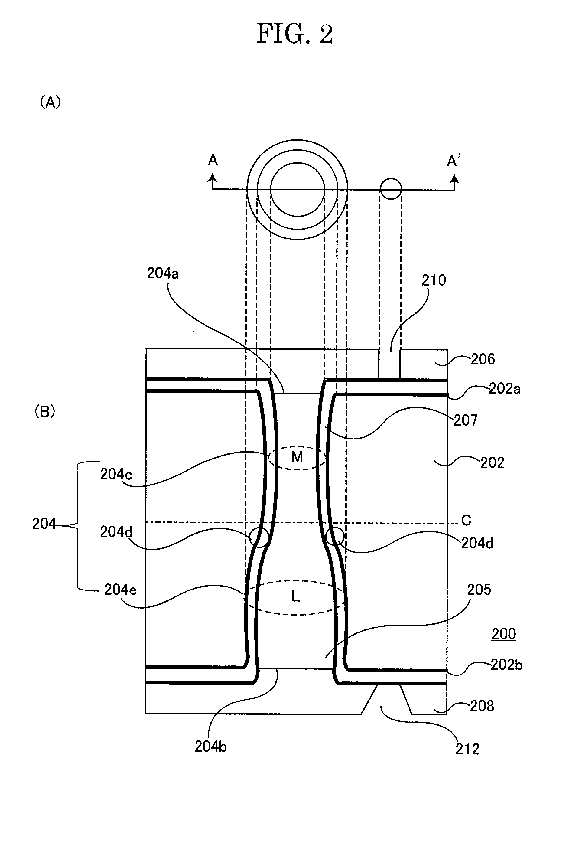
[0054]The structure of a through-hole electrode substrate 200 of the embodiment of the invention related to the present embodiment is explained while referring to FIG. 2. FIG. 2 (A) is a planar diagram of the through-hole electrode substrate 200 of the embodiment of the invention related to the present embodiment seen from the upper surface. FIG. 2 (B) is a cross-sectional diagram of the line A˜A′ in FIG. 2 (A). Both FIGS. 2 (A) and (B) show a part of the through-hole electrode substrate 200 of the embodiment of the invention related to the present embodiment for the convenience of explanation.

[0055]The through-hole electrode substrate 200 of the embodiment of the invention related to the present embodiment is arranged with a substrate 202, a through-hole 204, a filler 205, insulation layers 206 and 208, and via's 210 and 212. Furthermore, a wiring structure body and electronic components and the like may also be further mounted respectively on a first surface 202a and second surfac...

third embodiment

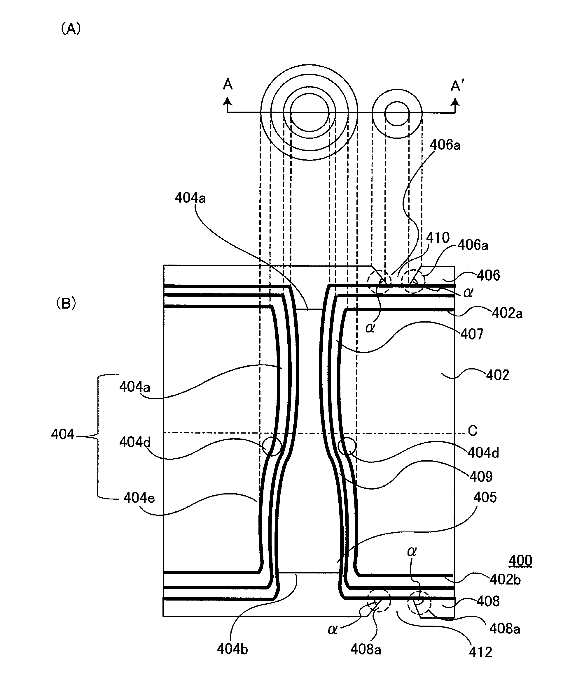
[0065]The structure of a through-hole electrode substrate 300 of the embodiment of the invention related to the present embodiment is explained while referring to FIG. 3. FIG. 3 (A) is a planar diagram of the through-hole electrode substrate 300 of the embodiment of the invention related to the present embodiment seen from the upper surface. FIG. 3 (B) is a cross-sectional diagram of the line A˜A′ in FIG. 3 (A). Both FIGS. 3 (A) and (B) show a part of the through-hole electrode substrate 300 of the embodiment of the invention related to the present embodiment for the convenience of explanation.

[0066]The through-hole electrode substrate 300 of the embodiment of the invention related to the present embodiment is arranged with a substrate 302, a through-hole 304, a filler 305, insulation layers 306 and 308, and via's 310 and 312. Furthermore, a wiring structure body and electronic components and the like may also be further mounted respectively on a first surface 302a and second surfac...


PUM


Abstract

A through-hole electrode substrate includes a substrate including a through-hole extending from a first aperture of a first surface to a second aperture of a second surface, an area of the second aperture being larger than that of the first aperture, the through-hole having a minimum aperture part between the first aperture and the second aperture, wherein an area of the minimum aperture part in a planer view is smallest among a plurality of areas of the through-hole in a planer view, a filler arranged within the through-hole, and at least one gas discharge member contacting the filler exposed to one of the first surface and the second surface.

Description

CROSS-REFERENCE TO RELATED APPLICATIONS[0001]This application is based upon and claims the benefit of priority from the prior Japanese Patent Application No. 2013-241392, filed on Nov. 21, 2013, and PCT Application No. PCT / JP2014 / 080649, filed on Nov. 19, 2014, the entire contents of which are incorporated herein by reference.FIELD[0002]The embodiment of the invention is related to a through-hole electrode substrate arranged with a through-hole electrode which passes through a top surface and rear surface of a substrate. In particular, the embodiment of the invention is related to a through-hole electrode substrate used as an interposer substrate for connecting a plurality of elements. In addition, the embodiment of the invention is related to a semiconductor device which uses the through-hole electrode substrate.BACKGROUND[0003]In recent years, the development of through-hole electrode substrates arranged with a conductive part which conducts a top surface and rear surface of a sub...

Claims


Application Information

Patent Timeline
IPC IPC(8): H01L23/498
CPCH01L23/49894H01L23/49827H01L23/13H01L25/065H01L25/18H05K1/115H05K3/28H05K3/445H05K2201/09154H05K2201/09563H05K2201/09581H05K2201/0959H05K2201/09854H05K2203/0594H01L2224/16145H01L2224/48091H01L2224/73257H01L23/481H01L23/15H01L2224/0401H01L2224/04042H01L2225/0651H01L2225/06517H01L2924/14H01L2924/1432H01L2924/1434H01L2924/1461H01L2225/06572H01L2224/16165H01L24/13H01L24/16H01L24/29H01L24/32H01L24/48H01L24/73H01L2224/13109H01L2224/13144H01L2224/13147H01L2224/16146H01L2224/16227H01L2224/2919H01L2224/32225H01L2224/48227H01L2224/81805H01L2224/8385H01L2924/15787H01L2924/15788H01L2924/1579H01L2924/381H01L2924/00014H01L2924/05432H01L2924/0665H01L2924/07025
Inventor KURAMOCHI, SATORUKOIWA, SUMIOYOSHIOKA, HIDENORI
Owner DAI NIPPON PRINTING CO LTD
Why Eureka
Try Eureka