Proximity luminance sensor and method for manufacturing same

a technology of luminance sensor and manufacturing method, which is applied in the direction of photometry using electric radiation detectors, optical radiation measurement, instruments, etc., can solve the problems of increasing the manufacturing cost of the housing, affecting the quality of the product, so as to reduce the optical interference phenomenon, reduce the manufacturing cost and manufacturing time, and prevent the effect of lens contamination or damag

Inactive Publication Date: 2016-10-20
ITM SEMICON CO LTD
View PDF4 Cites 3 Cited by
  • Summary
  • Abstract
  • Description
  • Claims
  • Application Information

AI Technical Summary

Benefits of technology

[0021]The proximity luminance sensor and the method of manufacturing the same according to the present invention is obtained by assembling a housing array to a printed circuit board array followed by the separation into individual proximity luminance sensors, and thus provides advantageous effects of preventing contamination or damage to lenses, decreasing the optical interference phenomenon, reducing the manufacturing cost and manufacturing time, and thus substantially improving productivity. In addition, the scope of the present invention is not limited to these effects.

Problems solved by technology

However, in the first conventional method of manufacturing a proximity luminance sensor, the light-emitting lens unit and the light-receiving lens unit may be contaminated by the opaque material during the molding of the blocking wall.
However, in the second conventional method of manufacturing a proximity luminance sensor, each of the individually separated printed circuit boards and each of the housings made of metal are manually assembled each other, thereby increasing the manufacturing cost of the housings, and thus substantially decreasing productivity.

Method used


Image

  • Proximity luminance sensor and method for  manufacturing same
  • Proximity luminance sensor and method for  manufacturing same
  • Proximity luminance sensor and method for  manufacturing same

Examples


Embodiment Construction

Technical Problem

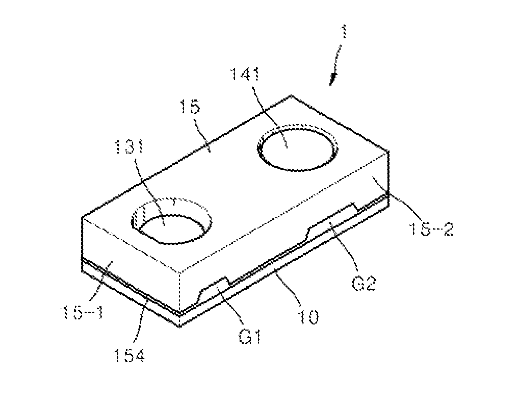
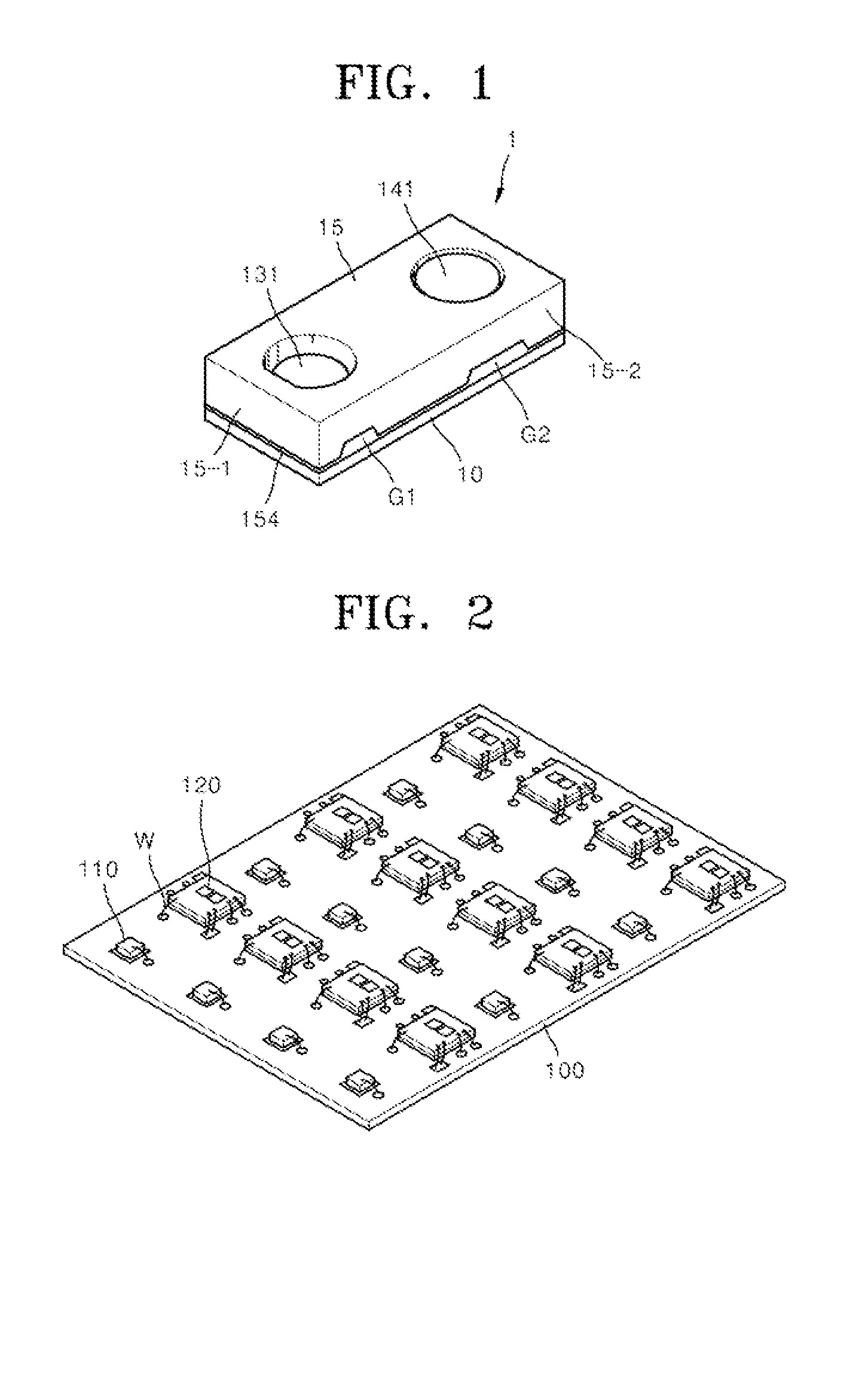
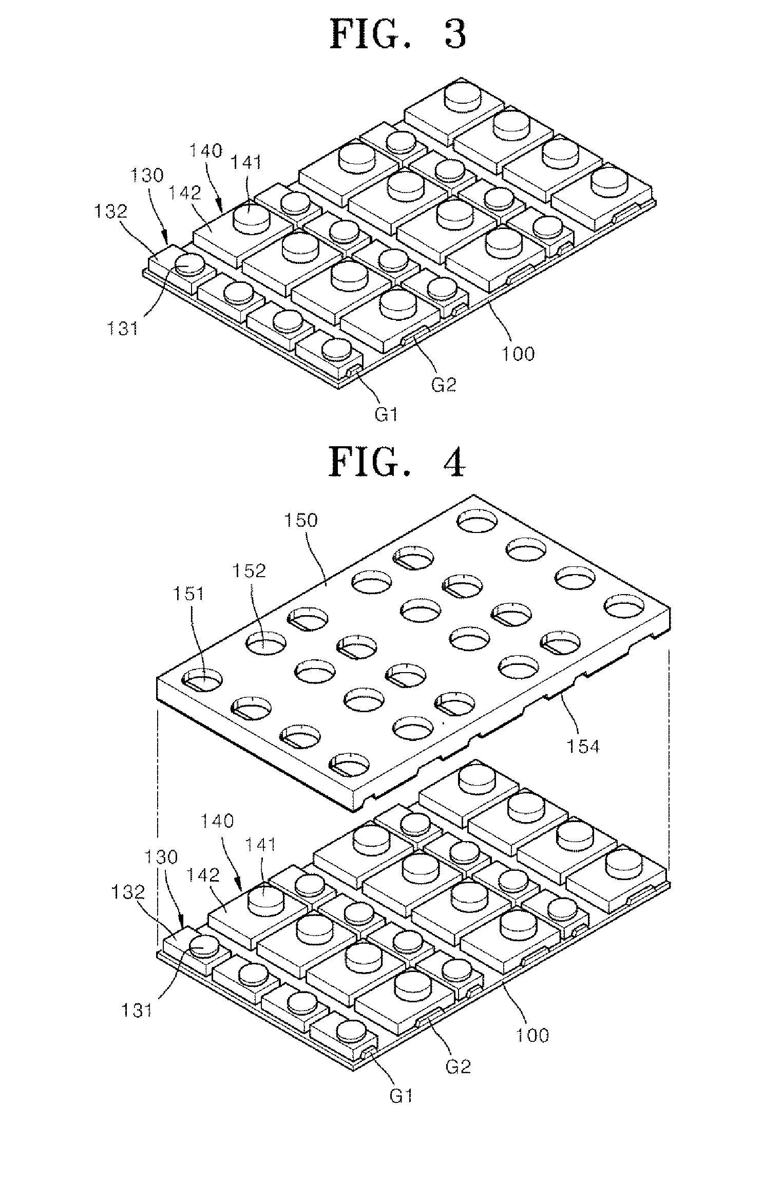
[0008]There are two conventional methods of manufacturing proximity luminance sensors.

[0009]In the first conventional method of manufacturing a proximity luminance sensor, a light-emitting lens unit and a light-receiving lens unit, both made of transparent material, are molded first on a light-emitting chip and a light-receiving chip in a printed circuit board array, respectively, and then a blocking wall made of opaque material is molded later so as to prevent crosstalk phenomenon in which a light generated from the light-emitting chip is directly transmitted to light-receiving chip.

[0010]However, in the first conventional method of manufacturing a proximity luminance sensor, the light-emitting lens unit and the light-receiving lens unit may be contaminated by the opaque material during the molding of the blocking wall.

[0011]In the second conventional method of manufacturing a proximity luminance sensor, a light-emitting lens unit and a light-receiving lens unit, b...


PUM


Abstract

The present invention relates to a proximity luminance sensor obtained by assembling a housing array to a printed circuit board array using an adhesive layer, prior to separation into individual proximity luminance sensors, thereby preventing contamination or damage to lenses, decreasing the optical interference phenomenon, reducing the manufacturing cost and manufacturing time, and thus substantially improving productivity. The proximity luminance sensor may comprise: a printed circuit board; a light-emitting chip mounted on the printed circuit board; a light-receiving chip mounted on the printed circuit board; a light-emitting lens unit surrounding the light-emitting chip; a light-receiving lens unit surrounding the light-receiving chip; a housing shaped to surround the light-emitting chip and the light-receiving chip and provided with a light-emitting window, which corresponds to the light-emitting lens unit, and a light-receiving window, which corresponds to the light-receiving lens unit; and an adhesive layer installed between the housing and the printed circuit board.

Description

TECHNICAL FIELD[0001]The present invention is related to a proximity luminance sensor and a method for manufacturing the same. In particular, the present invention relates to a proximity luminance sensor and a method for manufacturing the same, obtained by assembling a housing array to a printed circuit board array using an adhesive layer, prior to separation into individual proximity luminance sensors, thereby preventing contamination or damage to lenses, decreasing the optical interference phenomenon, reducing the manufacturing cost and manufacturing time, and thus substantially improving productivity.BACKGROUND ART[0002]A proximity luminance sensor is widely used for various motion sensing sensors or the like. The proximity luminance sensor can sense a reflected light generated from a light emitting unit such as an infrared emitting device and reflected from a subject, thereby sensing proximity of the subject or illumination of surroundings.[0003]There are two conventional method...

Claims


Application Information

Patent Timeline
Patent Type & Authority Applications(United States)
IPC IPC(8): G01J1/08H01L25/16H01L33/54H01L33/48H01L31/0232H01L31/16H01L33/62H01L31/02G01J1/44H01L33/58
CPCG01J1/08G01J1/44H01L25/167H01L33/54H01L33/58H01L31/02327H01L2933/005H01L31/16H01L33/62H01L31/02002H01L33/483H01L2933/0058H01L25/165H01L2224/48091H01L2224/48227H01L2924/00014G01J1/02
Inventor KIM, YUNG JUNGU, JA GUENLEE, SU SEOK
Owner ITM SEMICON CO LTD
Why Eureka
Try Eureka