Optical navigation chip, optical navigation module and optical encoder

a technology which is applied in the field of optical navigation module and optical encoder, can solve the problems of increasing the size the difficulty of simultaneously achieving high accuracy and microminiaturization of the optical encoder, and the error between the image captured by the sensing array and the actual imag

Active Publication Date: 2016-10-20
PIXART IMAGING INC
View PDF3 Cites 56 Cited by
  • Summary
  • Abstract
  • Description
  • Claims
  • Application Information

AI Technical Summary

Benefits of technology

[0011]To sum up, compared to the conventional optical encoder, the optical navigation chip, the optical navigation module and the optical encoder provided by the present disclosure do not need any optical lens disposed on the light-emitting unit and the sensing array, and the optical navigation chip, the optical navigation module and the optical encoder can calculate the relative displacement betw

Problems solved by technology

Then, there are errors between the image captured by the sensing array and the actual image.
However, as in the above descriptions, the conventional optical encoder needs the optical le

Method used


Image

  • Optical navigation chip, optical navigation module and optical encoder
  • Optical navigation chip, optical navigation module and optical encoder
  • Optical navigation chip, optical navigation module and optical encoder

Examples


Embodiment Construction

[0019]Reference will now be made in detail to the exemplary embodiments of the present disclosure, examples of which are illustrated in the accompanying drawings. Wherever possible, the same reference numbers are used in the drawings and the description to refer to the same or like parts.

[0020]Notably, the terms first, second, third, etc., may be used herein to describe various elements, but these elements should not be affected by such terms. Such terminology is used to distinguish one element from another. Further, the term “or” as used herein may include any one or combinations of the associated listed items.

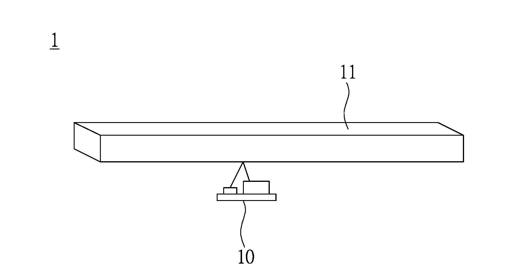
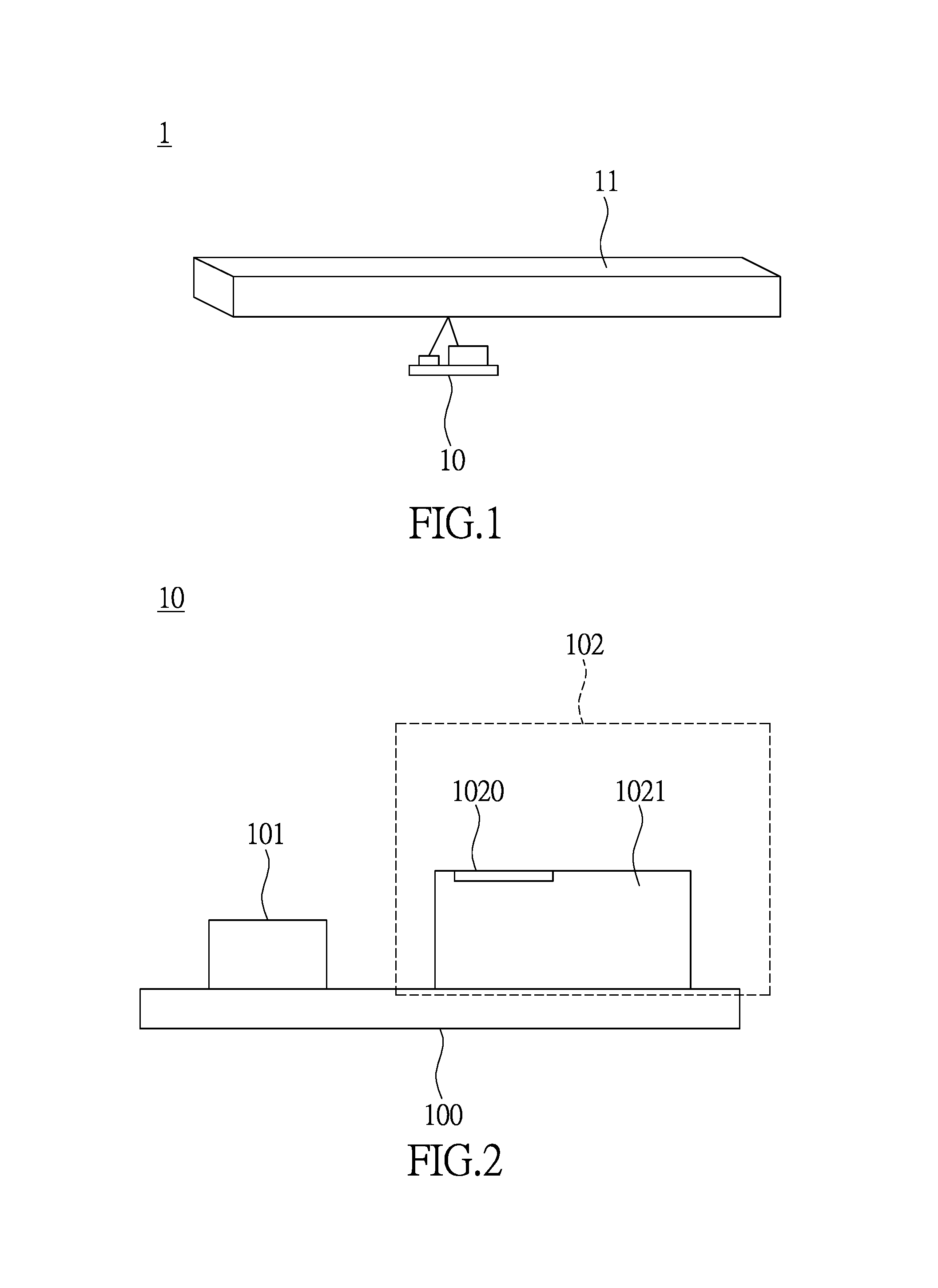
[0021]Please refer to FIG. 1, which is a schematic diagram illustrating an optical encoder according to an embodiment of the present disclosure. The optical encoder 1 includes an optical navigation module 10 and a displacement generating unit 11. The optical navigation module 10 is disposed corresponding to a surface of the displacement generating unit 11.

[0022]The optical na...


PUM


Abstract

The present disclosure illustrates an optical navigation chip. The optical navigation chip is disposed on an optical navigation module. The optical navigation module includes a light-emitting unit. The light-emitting unit provides a light beam to irradiate a surface of a displacement generating unit. The light beam has a low divergence angle to reduce scattering. The optical navigation chip includes a sensing array and a displacement calculating unit. The sensing array is disposed corresponding to the surface. The sensing array receives a reflected light beam which the surface reflects, and captures an image once every capturing interval based upon the reflected light beam. The displacement calculating unit calculates a relative displacement between the optical navigation chip and the surface according to the images.

Description

BACKGROUND[0001]1. Technical Field[0002]The present disclosure relates to an optical navigation chip, in particular, to a microminiaturization optical navigation chip, an optical navigation module having the optical navigation chip and an optical encoder.[0003]2. Description of Related Art[0004]Following the technology, more and more electronic devices have an optical navigation function. An optical encoder having the optical navigation function usually disposes an optical navigation chip to perform the optical navigation function. For example, the most common optical encoder is an optical mouse.[0005]The current optical mouse usually includes a light-emitting unit and the optical navigation chip. The light-emitting unit is configured for operatively providing a light beam to irradiate an object (such as a desktop). The optical navigation chip includes a sensing array. The sensing array is disposed corresponding to a surface of the object for receiving a reflected light beam reflect...

Claims


Application Information

Patent Timeline
IPC IPC(8): G06F3/0354G06F3/03
CPCG06F3/0304G06F3/03543G06F1/1652G06F3/0317
Inventor CHUNG, CHING-LINYANG, JR-SHENKE, CHIA-FUCHANG, YEN-MIN
Owner PIXART IMAGING INC
Why Eureka
Try Eureka