Electronic paper display device and manufacturing method thereof
- Summary
- Abstract
- Description
- Claims
- Application Information
AI Technical Summary
Benefits of technology
Problems solved by technology
Method used
Image

Examples
Embodiment Construction
[0029]Reference will now be made in detail to the present embodiments of the invention, examples of which are illustrated in the accompanying drawings. Wherever possible, the same reference numbers are used in the drawings and the description to refer to the same or like parts.
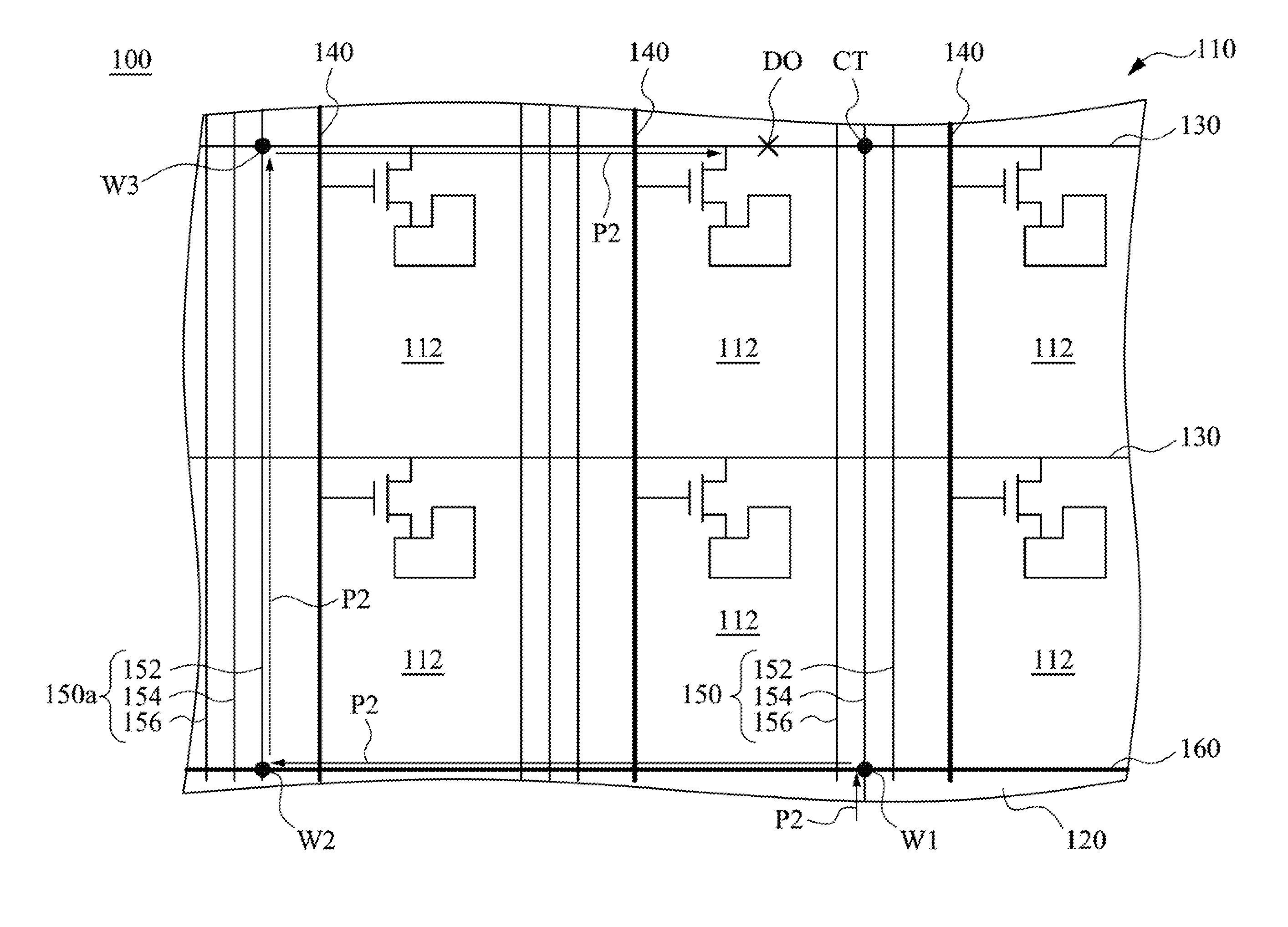
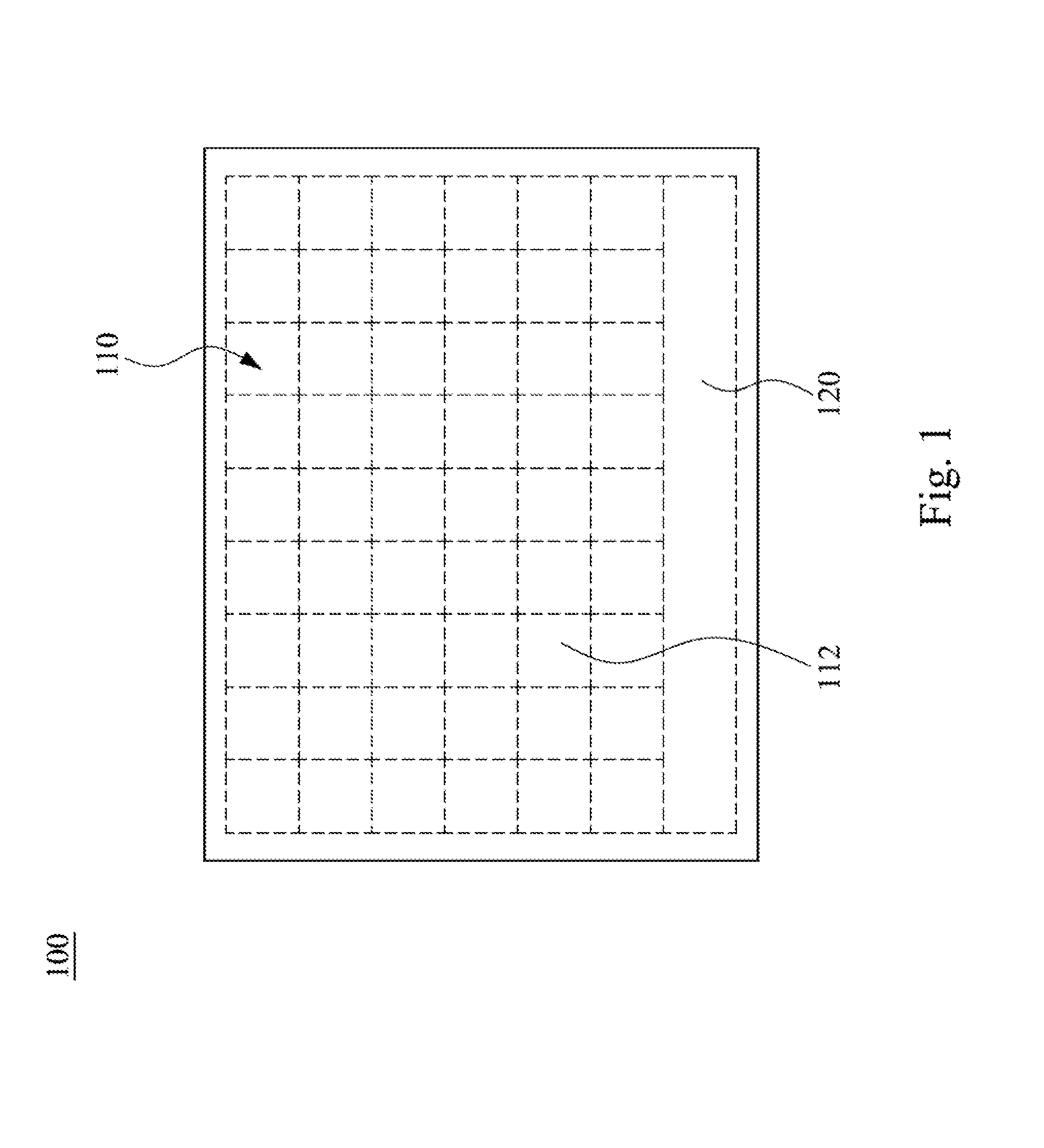
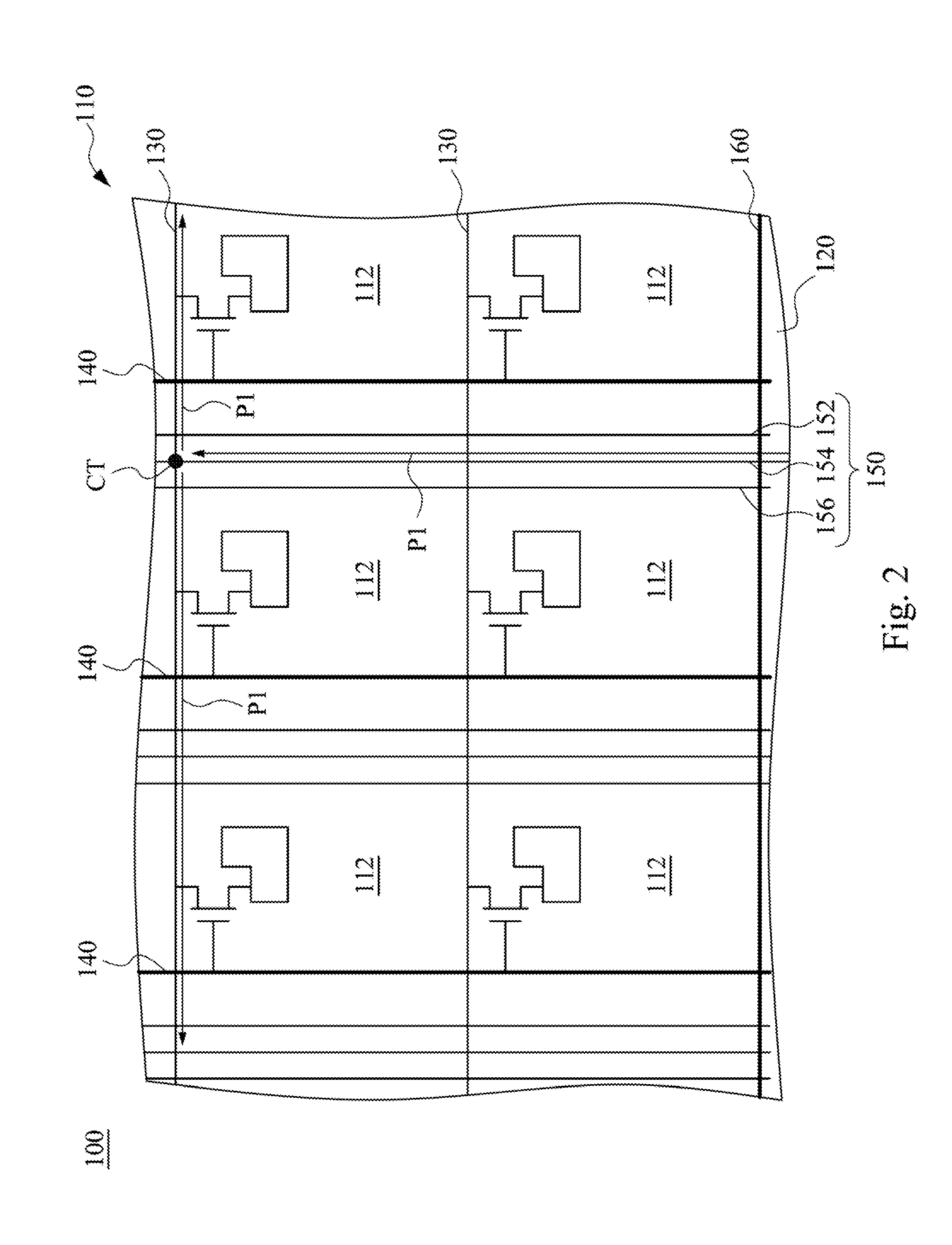
[0030]FIG. 1 is a top view of an electronic paper display device 100 according to one embodiment of the present invention. FIG. 2 is a partially enlarged view of the electronic paper display device 100 shown in FIG. 1. As shown in FIG. 1 and FIG. 2, the electronic paper display device 100 includes a display region 110, a signal-sending region 120, a plurality of data lines 130, a plurality of scan lines 140, a plurality of selection-line regions 150, and a repair line 160. The signal-sending region 120 is located at a side of the display region 110, which may be electrically connected to an integrated circuit (IC). The scan lines 140 intersect the data lines 130 to divide the display region 110 into plural pix...
PUM
| Property | Measurement | Unit |
|---|---|---|
| Electric potential / voltage | aaaaa | aaaaa |
Abstract
Description
Claims
Application Information
 - Generate Ideas
- Intellectual Property
- Life Sciences
- Materials
- Tech Scout
- Unparalleled Data Quality
- Higher Quality Content
- 60% Fewer Hallucinations
Browse by: Latest US Patents, China's latest patents, Technical Efficacy Thesaurus, Application Domain, Technology Topic, Popular Technical Reports.
© 2025 PatSnap. All rights reserved.Legal|Privacy policy|Modern Slavery Act Transparency Statement|Sitemap|About US| Contact US: help@patsnap.com