
OLED package structure and package method thereof

a package structure and packaging technology, applied in the field of display skill, can solve the problems of easy bending of the panel to influence the display effect, easy breakage, and inconvenient laser sealing technology, so as to prevent the issue of display uneven brightness, prevent bending or crushing of the package structure, and increase the bonding area

Inactive Publication Date: 2016-11-24
TCL CHINA STAR OPTOELECTRONICS TECH CO LTD
View PDF6 Cites 9 Cited by
  • Summary
  • Abstract
  • Description
  • Claims
  • Application Information

AI Technical Summary

Benefits of technology

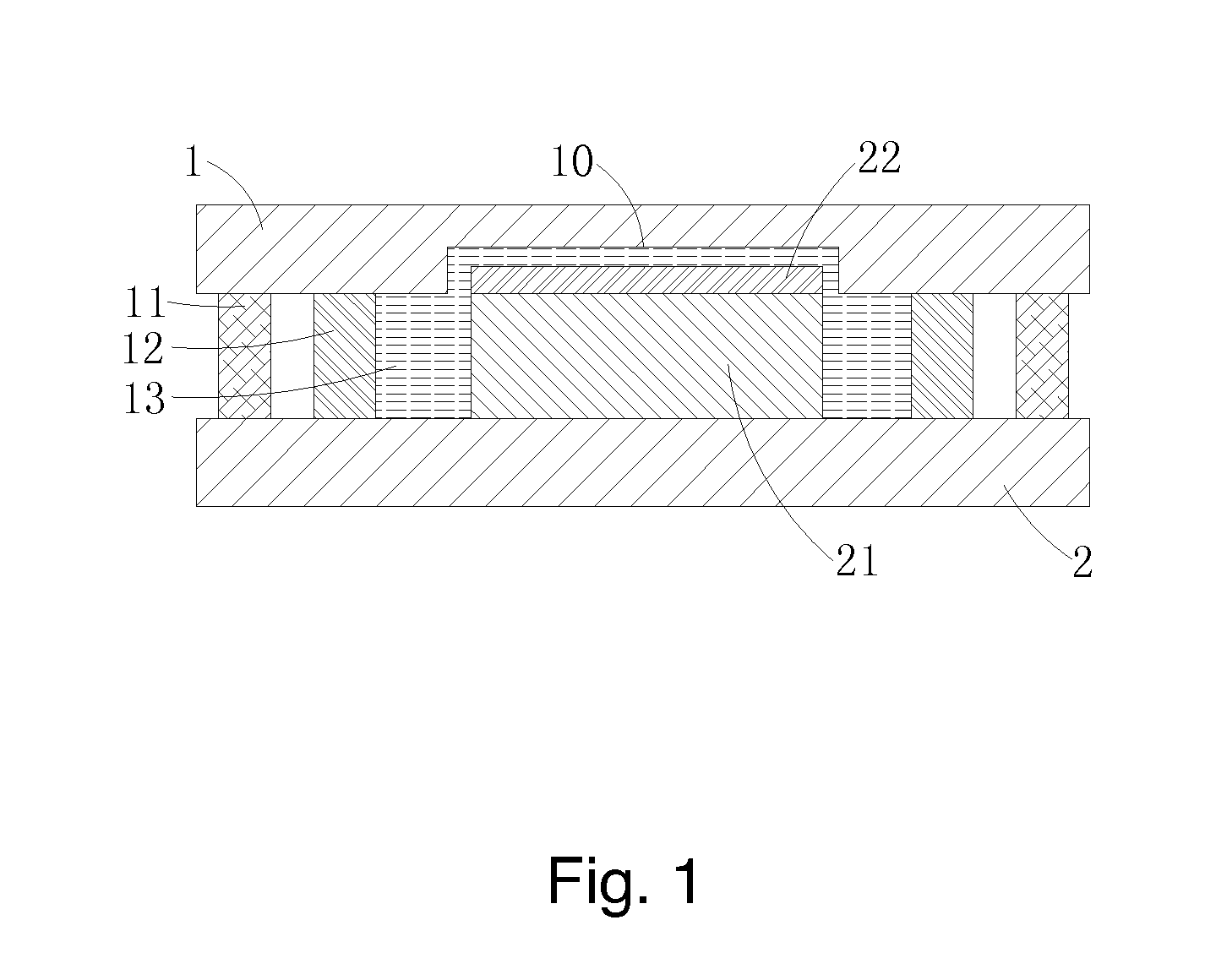
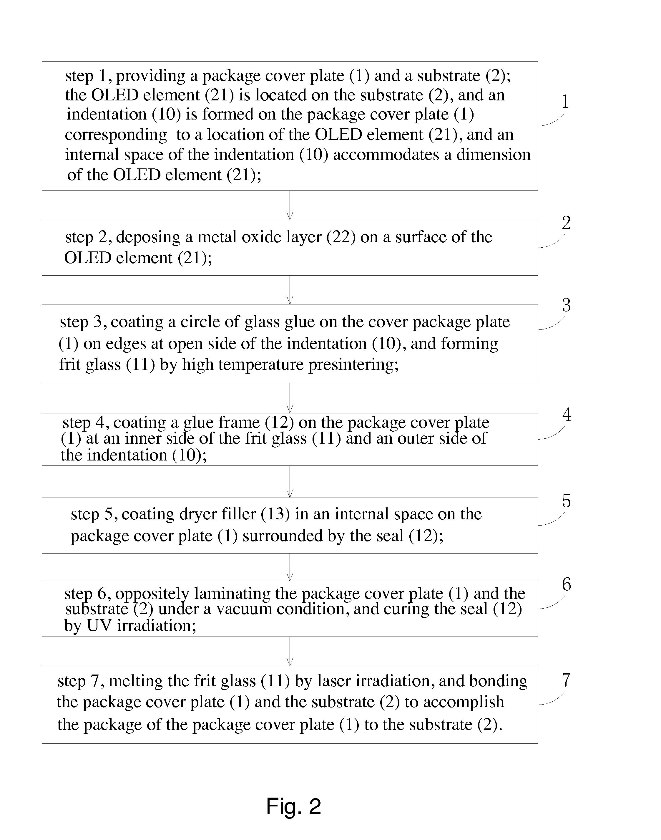
The present invention relates to an OLED package structure and method utilizing seal and frit glass to implement the package. A dryer filler is filled inside the seal for better tightness and mechanical strength. A metal oxide layer is formed on the surface of the OLED element to prevent display uneven brightness caused by corrosion of the dryer filler. This package structure and method can increase the bonding area of the package cover plate and substrate, promote tightness and mechanical strength, and prevent the issue of display uneven brightness.

Problems solved by technology

However, the laser sealing technology is not suitable for the large scale panels because the gaps exist in the panel, and the panel can be easily bent to influence the display effect and easily broken.

Method used


Image

  • OLED package structure and package method thereof
  • OLED package structure and package method thereof
  • OLED package structure and package method thereof

Examples


Embodiment Construction

[0039]For better explaining the technical solution and the effect of the present invention, the present invention will be further described in detail with the accompanying drawings and the specific embodiments.

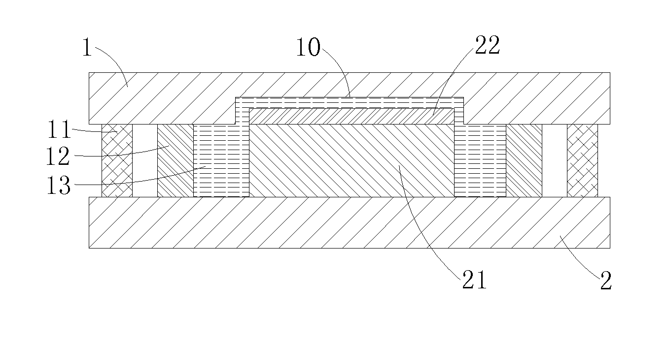
[0040]As shown in FIG. 1, the present invention provides an OLED package structure, comprising a package cover plate 1, a substrate 2, oppositely positioned with the package cover plate 1, an OLED element 21, positioned between the package cover plate 1 and the substrate 2 and set on the substrate 2, a metal oxide layer 22 formed on a surface of the OLED element 21, seal 12, positioned at periphery of the OLED element 21 to bond the package cover plate 1 and the substrate 2, dryer filler 13, filling an internal space surrounded by the seal 12 between the package cover plate 1 and the substrate 2, and covering the OLED element 21 and frit glass 11, located at periphery of the seal 12 to bond the package cover plate and 1 the substrate 2.

[0041]Preferably, both the package cover ...


PUM


Abstract

The present invention provides an OLED package structure and a package method thereof, and the structure comprises a package cover plate, a substrate, oppositely positioned with the package cover plate, an OLED element, positioned between the package cover plate and the substrate and set on the substrate, a metal oxide layer, formed on a surface of the OLED element, seal, positioned at periphery of the OLED element to bond the package cover plate and the substrate, dryer filler, filling an internal space surrounded by the seal between the package cover plate and the substrate, and covering the OLED element and frit glass, located at periphery of the seal to bond the package cover plate and the substrate, and the structure utilizes the seal and the frit glass to implement the package, and meanwhile, the dryer filler is filled inside the seal to make the package structure possess well tightness and mechanical strength, and a metal oxide layer is formed on a surface of the OLED element inside to prevent the issue of display uneven brightness caused by the corrosion of the dryer filler, particularly the liquid dryer to the lighting element.

Description

FIELD OF THE INVENTION[0001]The present invention relates to a display skill field, and more particularly to an OLED package structure and a package method thereof.BACKGROUND OF THE INVENTION[0002]OLED is an Organic Light Emitting Diodes Display possessing properties of self-illumination, high brightness, wide view angle, high contrast, flexibility and low power consumption, etc., and accordingly has been received more attentions. As being the display of next generation, it has been gradually replaced traditional liquid crystal displays and widely applied in cellular phone screens, computer displays, full color TV, etc. OLED display technology is different from the traditional liquid crystal display technology and the back light is not required. It utilizes an ultra thin organic material coating layer and a glass substrate, and theses organic material will illuminate when the current is conducted. Because the organic material can easily react with water and oxygen, the OLED display ...

Claims


Application Information

Patent Timeline
Patent Type & Authority Applications(United States)
IPC IPC(8): H01L51/52H01L51/56
CPCH01L51/5246H01L51/56H01L51/5259H01L51/5253H10K50/8426H10K50/846H10K2102/00H10K71/00H10K50/844
Inventor ZENG, WEIJINGWANG, YIFAN
Owner TCL CHINA STAR OPTOELECTRONICS TECH CO LTD
Learn More