Array substrate and liquid crystal display including the same

a liquid crystal display and substrate technology, applied in the field of array substrate and liquid crystal display, can solve the problems of leakage of light in the adjacent pixel, and achieve the effects of reducing the gap between pixels, and increasing the alignment stability of liquid crystals

Active Publication Date: 2016-12-01
SAMSUNG DISPLAY CO LTD
View PDF1 Cites 12 Cited by
  • Summary
  • Abstract
  • Description
  • Claims
  • Application Information

AI Technical Summary

Benefits of technology

[0008]In order to increase the alignment stability of liquid crystals in which a fringe field is formed, a structure in which a middle part of the finger-shaped pixel electrode protrudes toward a neighboring pixel area has been suggested. However, as the resolution of liquid crystal displays (“LCDs”) increases, a gap between pixels is reduced. Therefore, a pixel electrode having a protruding middle part affects liquid crystals in an adjacent pixel, thereby causing the leakage of light in the adjacent pixel.
[0009]Exemplary embodiments of the invention provide an array substrate which can increase the alignment stability of liquid crystals and prevent the leakage of light in an adjacent pixel.
[0010]Exemplary embodiments of the invention also provide an LCD which can increase the alignment stability of liquid crystals and prevent the leakage of light in an adjacent pixel.

Problems solved by technology

Therefore, a pixel electrode having a protruding middle part affects liquid crystals in an adjacent pixel, thereby causing the leakage of light in the adjacent pixel.

Method used


Image

  • Array substrate and liquid crystal display including the same
  • Array substrate and liquid crystal display including the same
  • Array substrate and liquid crystal display including the same

Examples


Embodiment Construction

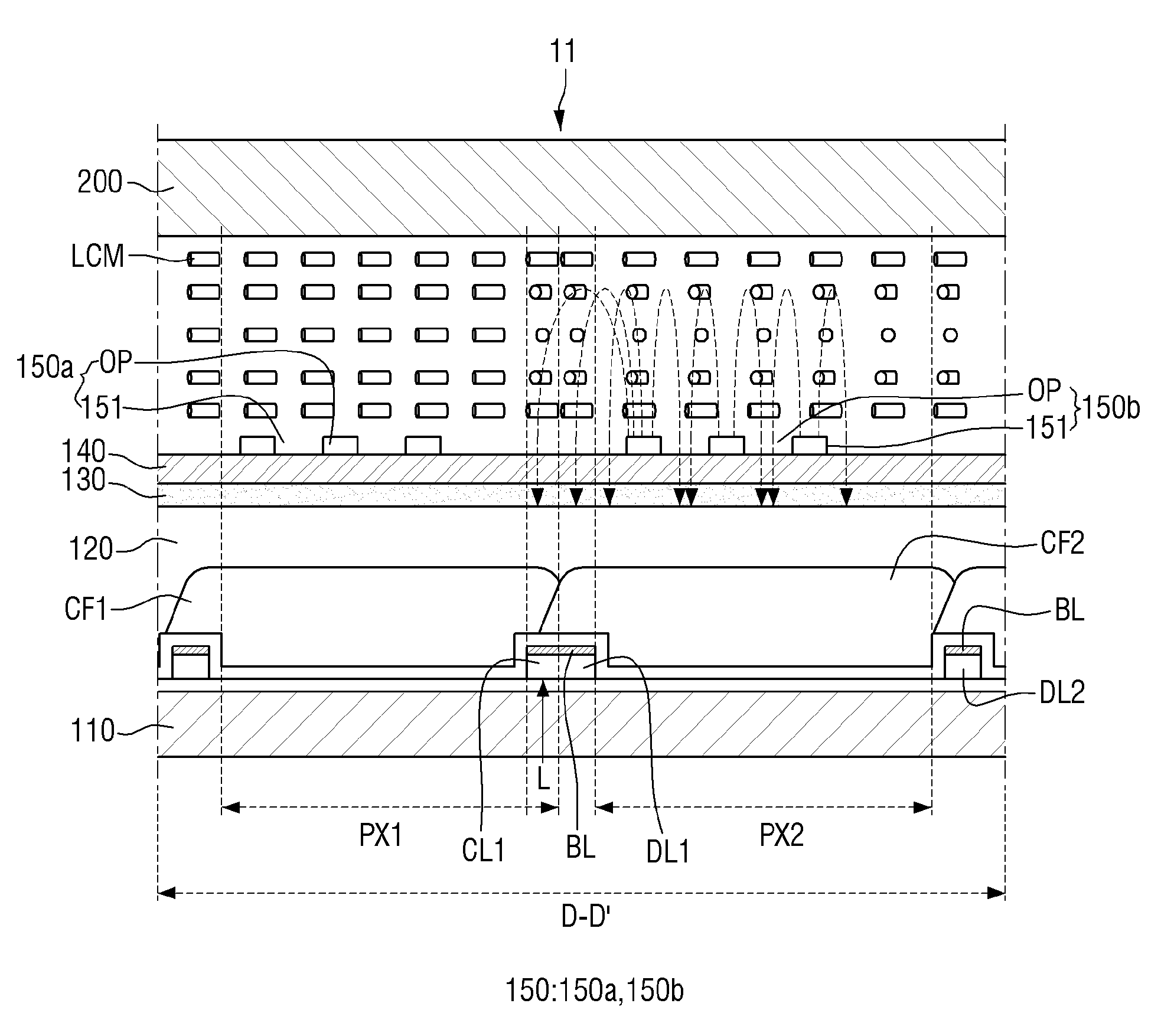
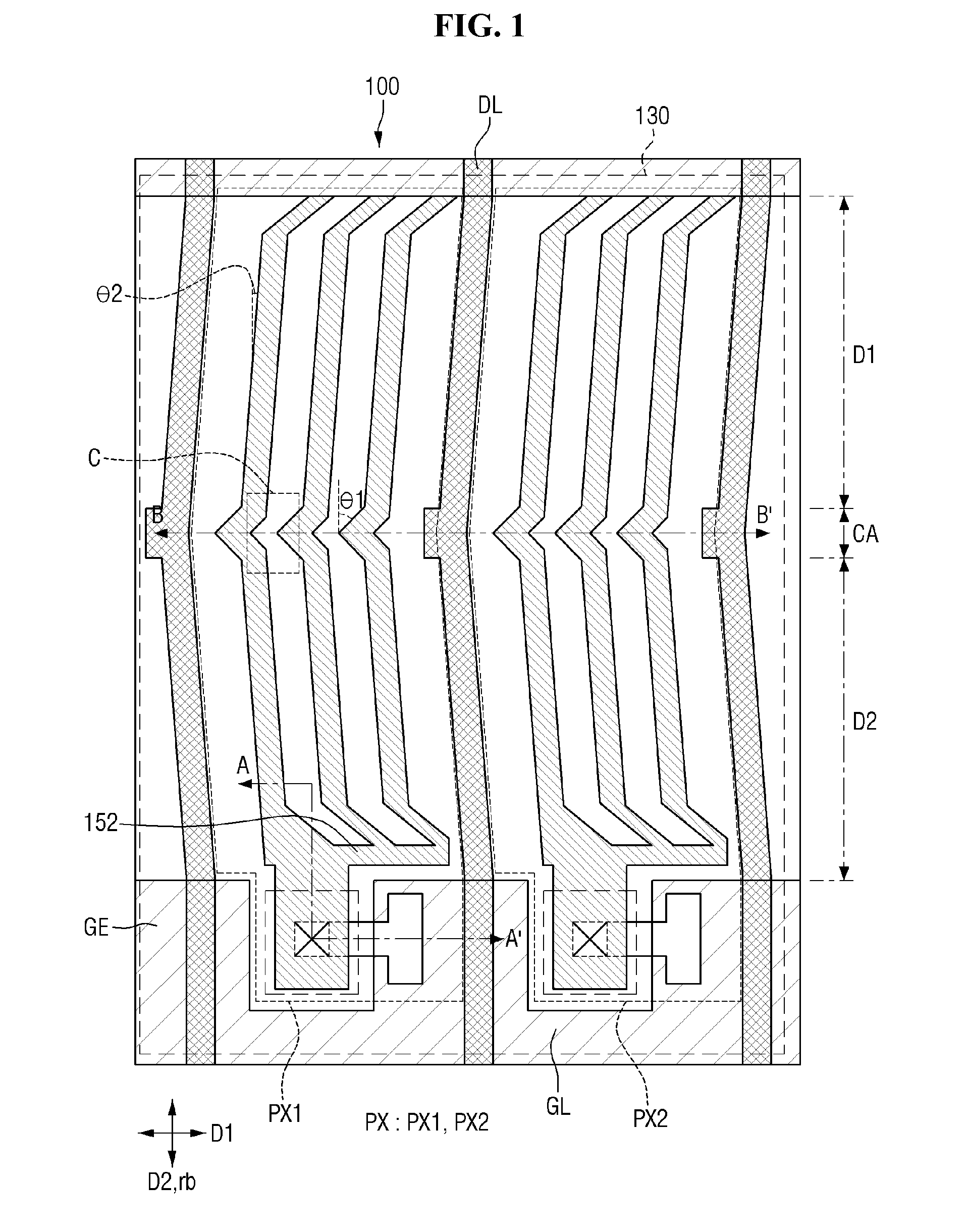
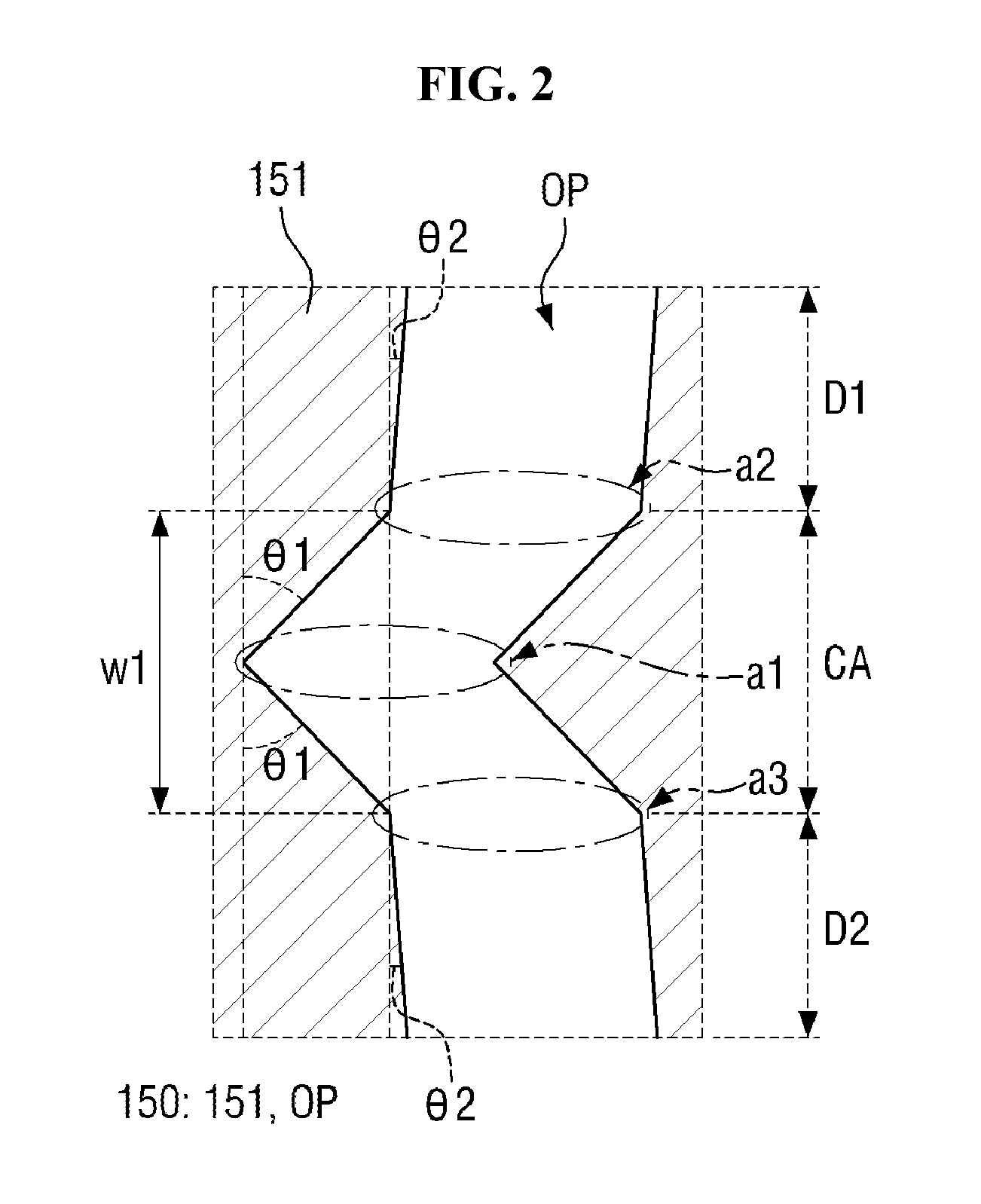
[0039]Advantages and features of the invention and methods of accomplishing the same may be understood more readily by reference to the following detailed description of preferred embodiments and the accompanying drawings. The invention may, however, be embodied in many different forms and should not be construed as being limited to the embodiments set forth herein. Rather, these embodiments are provided so that this disclosure will be thorough and complete and will fully convey the concept of the invention to those skilled in the art, and the invention will only be defined by the appended claims. Like reference numerals refer to like elements throughout the specification.

[0040]The terminology used herein is for the purpose of describing particular embodiments only and is not intended to be limiting of the invention. As used herein, the singular forms “a”, “an” and “the” are intended to include the plural forms as well, unless the context clearly indicates otherwise. It will be furt...


PUM

PropertyMeasurementUnit
angle θ1aaaaaaaaaa
angle θ1aaaaaaaaaa
angle θ1aaaaaaaaaa

Abstract

Array substrate includes a gate line which extends along a first direction, a gate insulating layer which covers the gate line, a data line located on the gate insulating layer and intersects the gate line, a thin-film transistor (“TFT”) which has a control electrode connected to the gate line and an electrode connected to the data line, a pixel electrode connected to the other electrode of the TFT, where the pixel electrode includes branch electrodes, openings are defined between the branch electrodes, each of the openings includes a first bent portion which corresponds to a middle part of the pixel area and a second bent portion and a third bent portion located symmetrically to each other with respect to the first bent portion, and the data line includes a cover region which protrudes toward the pixel area and covers at least part of the pixel area.

Description

[0001]This application claims priority to Korean Patent Application No. 10-2015-0073681 filed on May 27, 2015 and all the benefits accruing therefrom under 35 U.S.C. §119, the content of which in its entirety is incorporated herein by reference.BACKGROUND[0002]1. Field[0003]The invention relates to an array substrate and a liquid crystal display (“LCD”) having the same.[0004]2. Description of the Related Art[0005]Liquid crystal displays (“LCDs”) consume low power due to low operating voltage and are portable. Due to these advantages, LCDs are applied in a wide variety of fields including notebook computers, monitors, spaceships, and airplanes. An LCD includes a lower substrate, an upper substrate, and a liquid crystal layer formed between the two substrates. In the LCD, the arrangement of liquid crystal molecules in the liquid crystal layer is controlled according to whether an electric field is applied to the liquid crystal layer, and the transmittance of light is thereby controlle...

Claims


Application Information

Patent Timeline
Patent Type & Authority Applications(United States)
IPC IPC(8): G02F1/1362G02F1/1333G02F1/1343H01L27/12G02F1/1368
CPCG02F1/136286H01L27/1244G02F2001/13629G02F1/134309G02F1/133345G02F1/1368G02F1/136209G02F1/13629
Inventor PARK, SEUNG HYUNSONG, JEAN HO
Owner SAMSUNG DISPLAY CO LTD
Why Eureka
Try Eureka