Photo sensor module

a technology of photo sensor and module, which is applied in the field of photo sensor, can solve the problems of difficult to reduce the size of the uv sensor, the inability of the uv sensor to perform high sensitivity sensing functions, and the size of the ic chip comprising the uv sensor is difficult to reduce the size of the smart phone or wearable device, etc., and achieves the effect of improving the structure and reducing the size of the equipped ic chip

Inactive Publication Date: 2016-12-29
ATRIA TECH INC
View PDF3 Cites 0 Cited by
  • Summary
  • Abstract
  • Description
  • Claims
  • Application Information

AI Technical Summary

Benefits of technology

[0013]The present disclosure minimizes size of an IC chip size by improving a structure forming a passive device perpendicular to a UV sensor.
[0037]The following description discloses a UV sensor that senses UV and a logic section that processes the UV sensor sensed signal simultaneously, on a semiconductor substrate. For example, when forming a poly silicon layer by deposing poly silicon on a field oxide layer or when forming a photo diode by doping impurity on the poly silicon layer, devices can be comprised under the identical process as the identical process is also applied together on a logic section. Therefore, the following description discloses a UV sensor that not only reduces the manufacture cost but also simplifies the manufacture process.
[0039]Additionally, the following description discloses a UV sensor that can not only place an active device or a passive device on a lower UV sensor but can also improved a structure by placing a sensor section that can sense non-UV. Thus, a UV sensor can reduce an equipped IC chip size.

Problems solved by technology

This makes it difficult to reduce the size of an IC chip comprising a UV sensor and making it difficult to reduce the size of the smart phones or wearable devices smaller.
The UV sensors known in the art are not capable of high sensitivity sensing function and being cheaper than a SOI substrate.

Method used


Image

  • Photo sensor module
  • Photo sensor module
  • Photo sensor module

Examples


Embodiment Construction

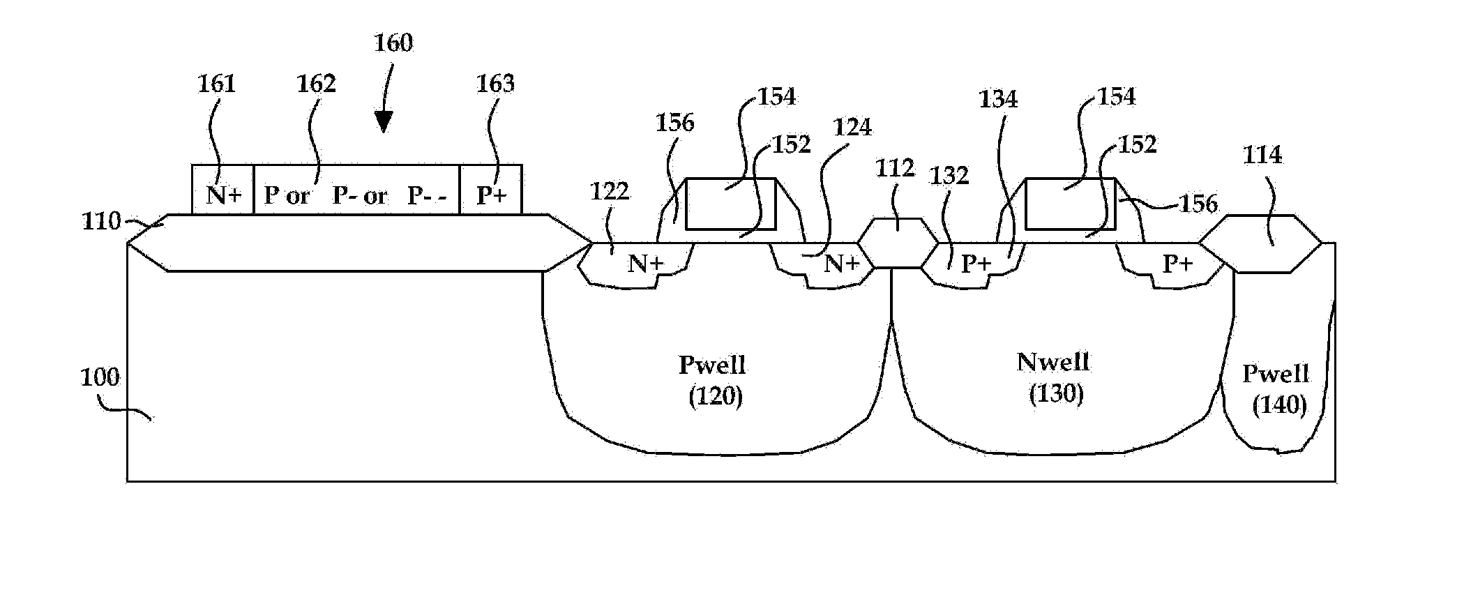
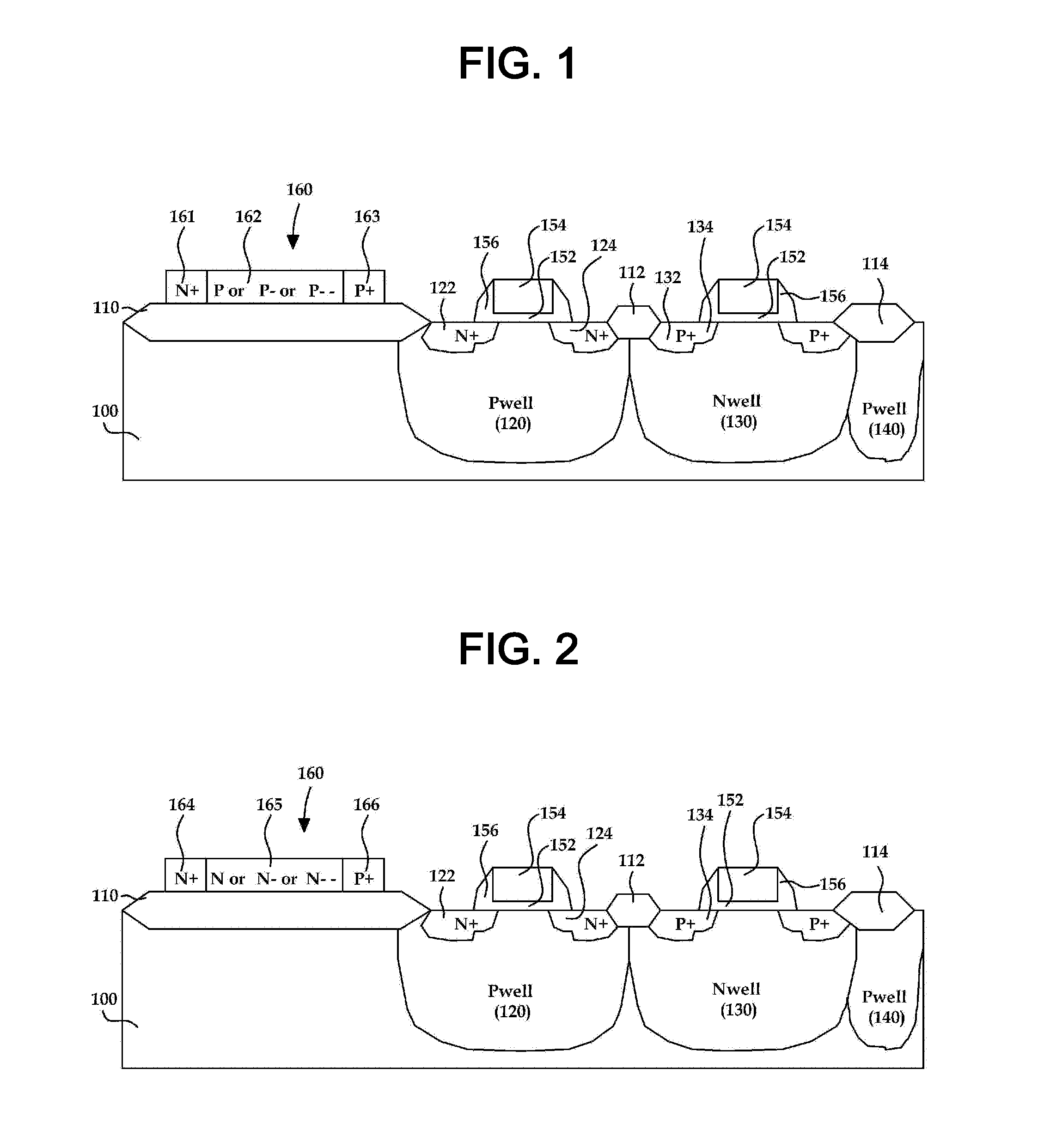
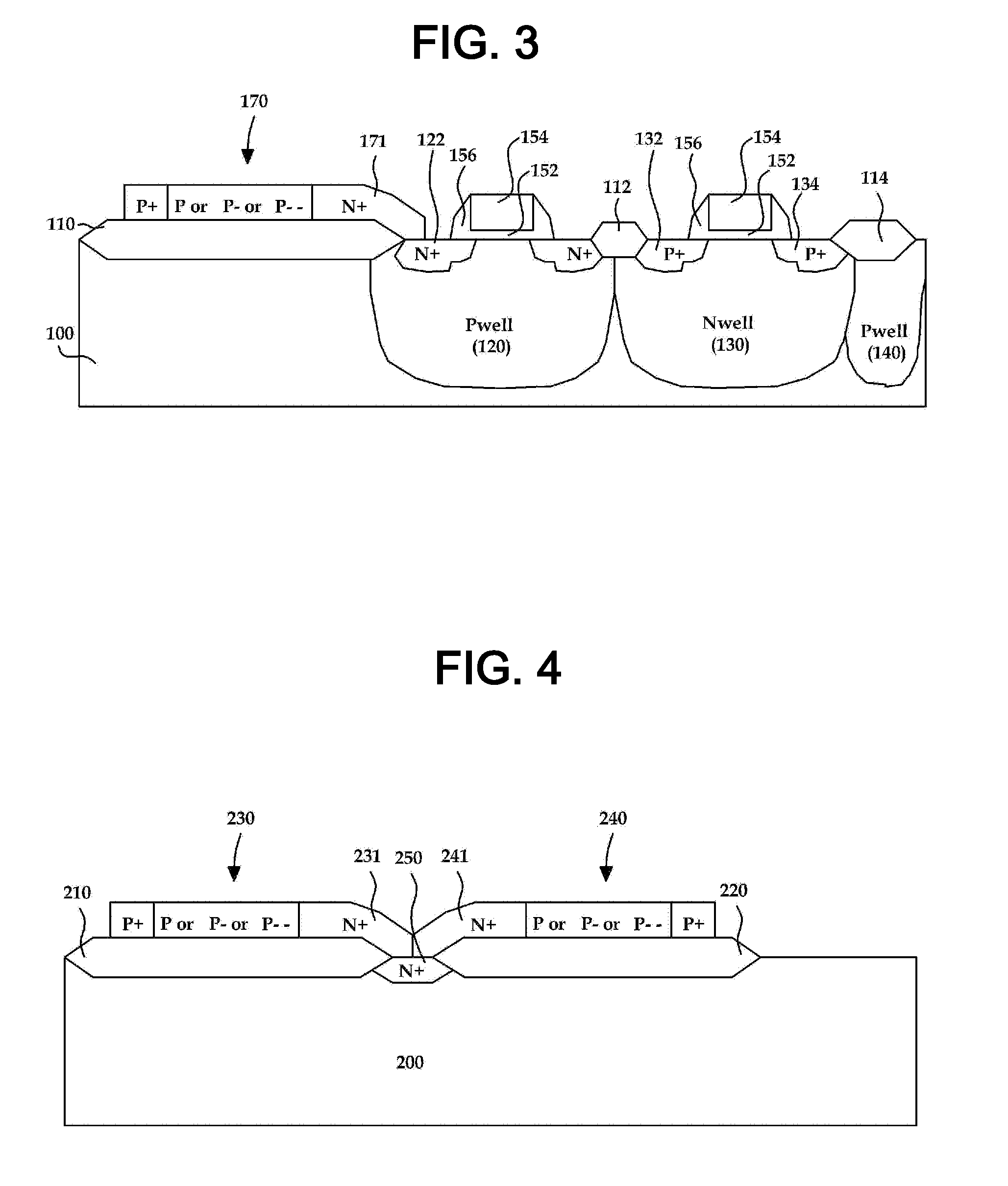
[0055]The following detailed description is provided to assist the reader in gaining a comprehensive understanding of the methods, apparatuses, and / or systems described herein. However, various changes, modifications, and equivalents of the systems, apparatuses and / or methods described herein will be apparent to one of ordinary skill in the art. The progression of processing steps and / or operations described is an example; however, the sequence of operations is not limited to that set forth herein and may be changed as is known in the art, with the exception of steps and / or operations necessarily occurring in a certain order. Also, descriptions of functions and constructions that are well known to one of ordinary skill in the art may be omitted for increased clarity and conciseness.

[0056]The features described herein may be embodied in different forms, and are not to be construed as being limited to the examples described herein. Rather, the examples described herein have been provi...


PUM


Abstract

The present disclosure relates to a photo sensor module. The thickness and size of an IC chip may be reduced by manufacturing a photo sensor based on a semiconductor substrate and improving the structure to place a UV sensor on the upper section of an active device or a passive device. The photo sensor module includes a semiconductor substrate, a field oxide layer, formed on the semiconductor substrate, and a photo sensor comprising a photo diode formed on the field oxide layer.

Description

CROSS-REFERENCE TO RELATED APPLICATIONS[0001]This application is a divisional of U.S. patent application Ser. No. 14 / 796,050 filed on Jul. 10, 2015, which claims the benefit under 35 USC 119(a) of Korean Patent Application No. 10-2014-0107936 filed on Aug. 19, 2014 in the Korean Intellectual Property Office, the entire disclosure of which is incorporated herein by reference for all purposes.BACKGROUND[0002]1. Field[0003]The following description relates to a photo sensor and to a photo sensor module configuring a UV sensor using poly silicon formed on a semiconductor substrate, which minimizes size of a chip by forming a passive device processing sensing signal in a vertical direction with a UV sensor.[0004]2. Description of Related Art[0005]UV sensing has recently been incorporated in various portable products, such as, for example, smart phone and wearable devices, because of an increase in awareness of protecting people from UV exposure. Such products, which are equipped with a U...

Claims


Application Information

Patent Timeline
Patent Type & Authority Applications(United States)
IPC IPC(8): H01L27/144H01L31/0216H01L31/103H01L31/02H01L31/0368H01L31/0392
CPCH01L27/1443H01L31/03682H01L31/02164H01L31/103H01L31/02019H01L31/03921
Inventor HEBERT, FRANCOISCHOE, SEONG MIN
Owner ATRIA TECH INC
Why Eureka
Try Eureka