Method for packaging micromachined devices

a micro-machined device and packaging technology, applied in the direction of semiconductor devices, semiconductor/solid-state device details, electrical apparatus, etc., can solve the problems of poor process reliability, serious affecting the performance and vacuum level of mems products, and insufficient active space for motion devices, etc., to achieve good process reliability, good mechanical properties, good thermal conductivity

Inactive Publication Date: 2012-10-16
HUANG JUNG TANG
View PDF1 Cites 2 Cited by
  • Summary
  • Abstract
  • Description
  • Claims
  • Application Information

AI Technical Summary

Benefits of technology

[0012]The invention can simultaneously accomplish 0-level packaging and 1-level packaging by copper pillars to form the surrounding wall and signal conductors. The advantages of copper pillars contain: (1) good process reliability; (2) good mechanical properties; (3) good thermal conductivity; (4) Pb-free; (5) less risk of collapse during reflow process; (6) no deformation issues after packaging; (6) minimizing chip size.
[0013]The advantages of this invention include: (1) providing a packaging method for micromachined devices; (2) providing at least one chamber or active space for micromachined structures by bonding with the surrounding trench and wall; (3) avoiding collapse problems and reducing the risk of hurting micromachined devices by using copper pillars; (4) minimizing packaging size; (5) controlling vacuum pressure by high coplanarity of copper pillars for hermetically bonding two chips; (6) providing strong functions by integrating with micro controller unit (MCU) and copper pillar conductors on the carrier chip.

Problems solved by technology

The thickness of the adhesive layer usually is less than 4 micrometers, which cannot offer enough active space for motion devices such as gyro and actuator.
The drawbacks of BCB bonding include: (1) prone to collapse in dispensing process; (2) emitting volatile gases during curing process; thus lead to poor process reliability.
All of above drawbacks seriously affect the performances and the vacuum level of MEMS products.
Furthermore, BCB is not conductive and can not conduct signals or electric power or heat dissipation except for bonding the cap with micromachined structures on the purpose of protection.
These two methods have to work in high temperature and high pressure environment, which will damage the brittle MEMS devices and decrease the yield rates.
And equipments of Eutectic Bonding or Anodic Bonding equipment are very expensive, which will increase the process costs.
Generally, wirebond and flip chip are not suitable for fine pitch devices, and TVS has complex processes and high process costs.
The drawbacks of these known micromachined structures include, for example, (1) the size is too big; (2), a complicated process is required; and (3) a non-functional cap only for mechanical protection purpose is needed.
Besides, the long bonding wire can result in poor signal noise ratio and be confined to low frequency application.
Although the SOC technology can integrate circuits and micromachined structures in one chip, the fabrication and packaging process of the SOC are complicated.

Method used


Image

  • Method for packaging micromachined devices
  • Method for packaging micromachined devices
  • Method for packaging micromachined devices

Examples


embodiment 2

[0037]Referring to FIG. 3, it illustrates the process flow for micromachined devices with environmental exposure such as microphone, gas sensor, flow sensor, humidity sensor, gauge pressure sensor etc. In order to allow micromachined devices to detect physical or chemical quantities from environment, the surrounding trench 24 and surrounding wall 25 has to form vent holes 26, shown as FIG. 3(a) and FIG. 3 (b). The packaging processes are similar to Embodiment 1, shown as FIG. 3 (c) and FIG. 3 (d), except the plastic encapsulation process is canceled.

embodiment 3

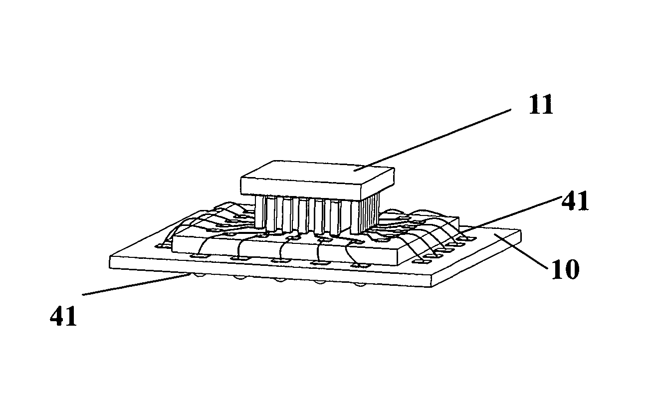
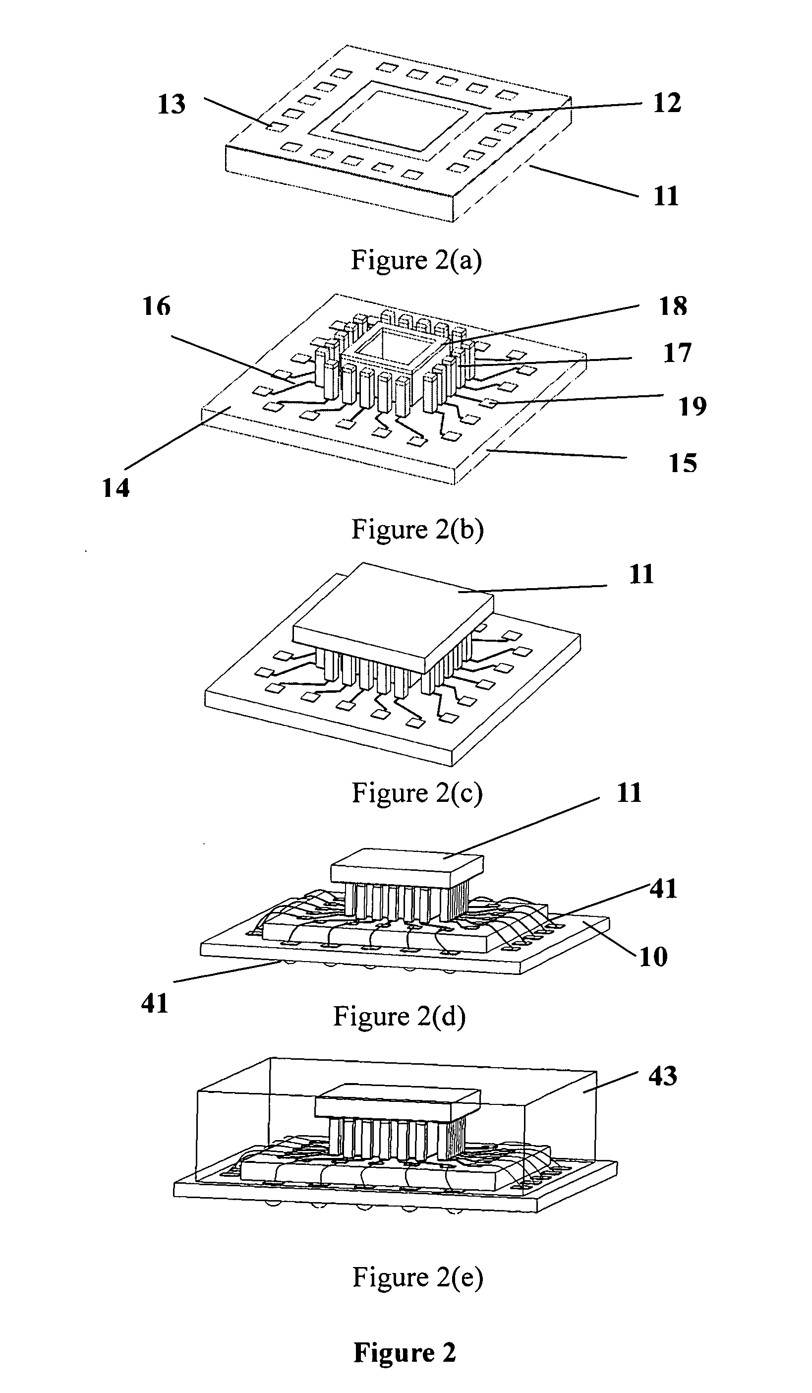
[0038]Referring to FIG. 4, in the above two examples, the pads 13 for wire bonding on the second chip 14 can also be connected to the backside of the second chip 14 by utilizing Through Silicon Via 17 (TSV) and then attaching solder balls or bumps 38 to directly become a fully packaged sensor or actuator. By deleting interposer 10, this embodiment can reduce volume and cost of micromachined products.

[0039]TSV technology has been applied in semiconductor industry several years and used to connect multiple ICs together in a package. The process of TSV comprises the following steps of: 1. forming through holes by using wet / dry etching technology or laser; 2. filling copper by electroforming. Electroforming is a common process, which soaks substrates in Cu bath with current. Furthermore, before filling through holes with Cu, deposing isolation layer and barrier layer are significant and seriously affect the performances of devices. Isolation layer is used to isolate Si-substrate and Cu ...

embodiment 4

[0040]Referring to FIG. 5, the second chip contains Micro Controller Unit 51(MCU), multiple surrounding continuous pads 52, corresponding to surrounding trench 12 on the first chip and at least three bump pads 53. One of the surrounding continuous pads 52 on the second chip is selected to be deposited into surrounding wall 18, which is corresponding to the surrounding trench 12 of the first chip and is depending on the size of the micromachined structures 54, shown as FIG. 5 (a). And bump pads 53 are also deposited into bump pillars 17 according to the signals or electric power required to I / O pad 19 of the first chip, shown as FIG. 5 (b). The advantages of embodiment 4 are that: (1) enhancing performances and forming the smart sensor by assembling MCU with the first chip; (2) providing the more flexible applications to different size of various micromachined structures 54, without redesigning the layout of MCU; (3) reducing the manufacturing cost. The packaging processes are simila...


PUM


Abstract

A method for packaging micromachined devices fabricated by MEMS and semiconductor process is disclosed in this invention. The method employed etching technique to etch a trench surrounding the micromachined components on each chip of the first wafer down to the bottom interconnection metal layer. The said trench can accommodate the solder of flip-chip packaging. On each chip of the second wafer, or called as the second chip, a surrounding copper pillar wall corresponding to the trench on the first chip is deposited. By wafer-level packaging, the trench on the first chip is aligned to the pillar wall, and then bonded together with elevated temperature. The face-to-face chamber formed between two chips can allow the movement of the micromachined structures. Further, the signal or power connections between two chips can be established by providing several discrete pillar bumps.

Description

FIELD OF INVENTION[0001]The present invention relates generally to the field of semiconductor manufacturing and Micro Electro Mechanical Systems (MEMS), or further extends to micromachined devices. More specifically, the present invention relates to methods for packaging of micromachined devices and other devices, and in some cases, devices that have nanomaterials, or devices that have multi-functions such as power system, MCU, antenna, RF, etc.DESCRIPTION OF RELATED ART[0002]The current packaging process for micromachined devices can separate into two parts, 0-level packaging and 1-level packaging.[0003]The 0-level packaging is using non-functional substrates such as pure silicon, glass, ceramic to be a cap and to seal the micromachined structures. The adhesive material between the cap and the micromachined structures are usually macromolecule components like Benzocyclobutane (BCB), gold and glass frit. The thickness of the adhesive layer usually is less than 4 micrometers, which c...

Claims


Application Information

Patent Timeline
Patent Type & Authority Patents(United States)
IPC IPC(8): H01L21/768H01L23/498
CPCB81B7/0077H01L25/165H01L2924/1461H01L2924/10253H01L2924/01322H01L2924/14H01L2924/09701H01L25/18H01L2224/32145H01L2224/48091H01L2224/48227H01L2225/06513H01L2924/01078H01L2924/01079H01L2924/00014H01L2924/00
Inventor HUANG, JUNG-TANGLIN, MING-JHEHSU, HOU-JUN
Owner HUANG JUNG TANG
Why Eureka
Try Eureka