Touch panel, display device, and touch panel manufacturing method
- Summary
- Abstract
- Description
- Claims
- Application Information
AI Technical Summary
Benefits of technology
Problems solved by technology
Method used
Image
Examples
first embodiment
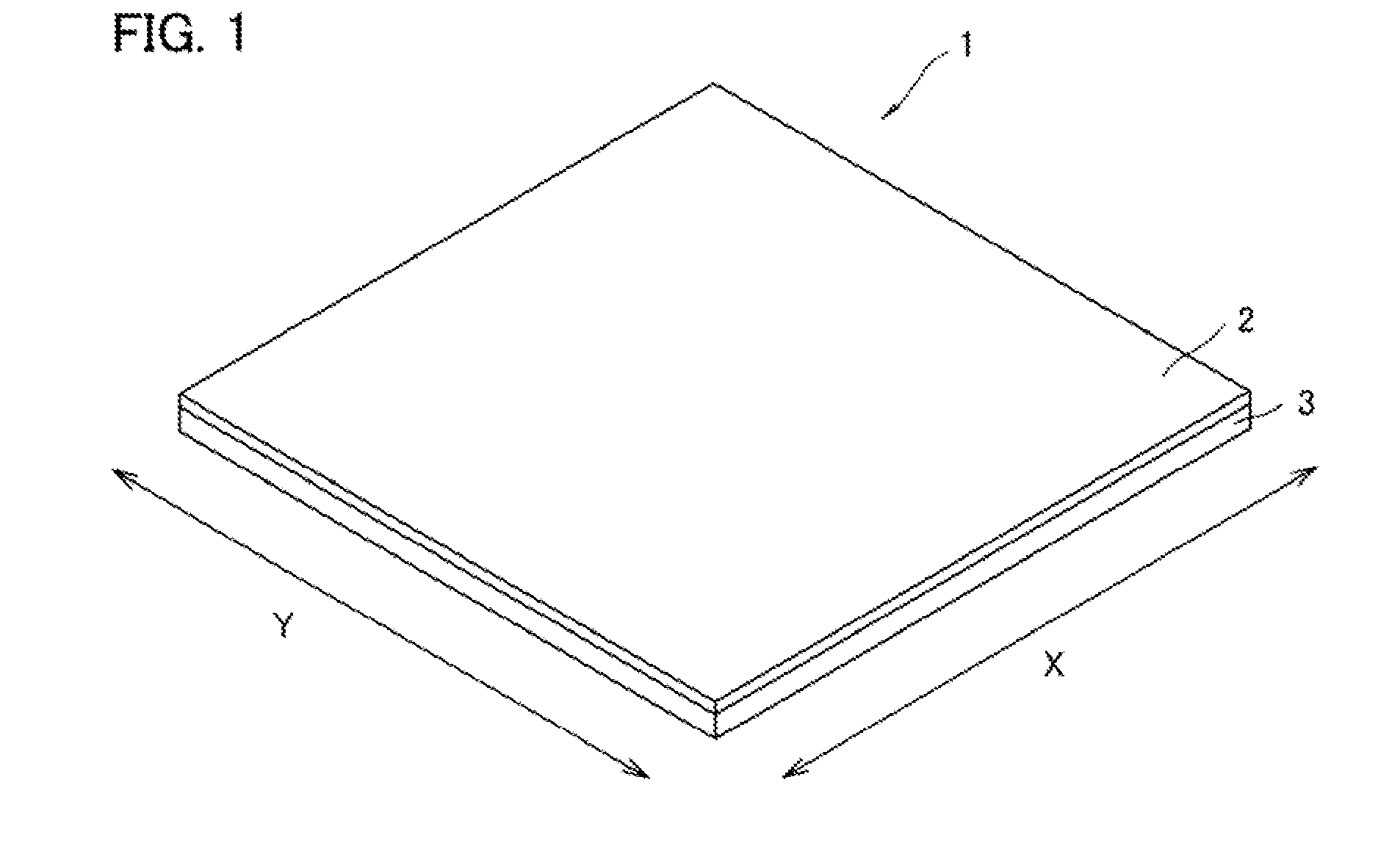
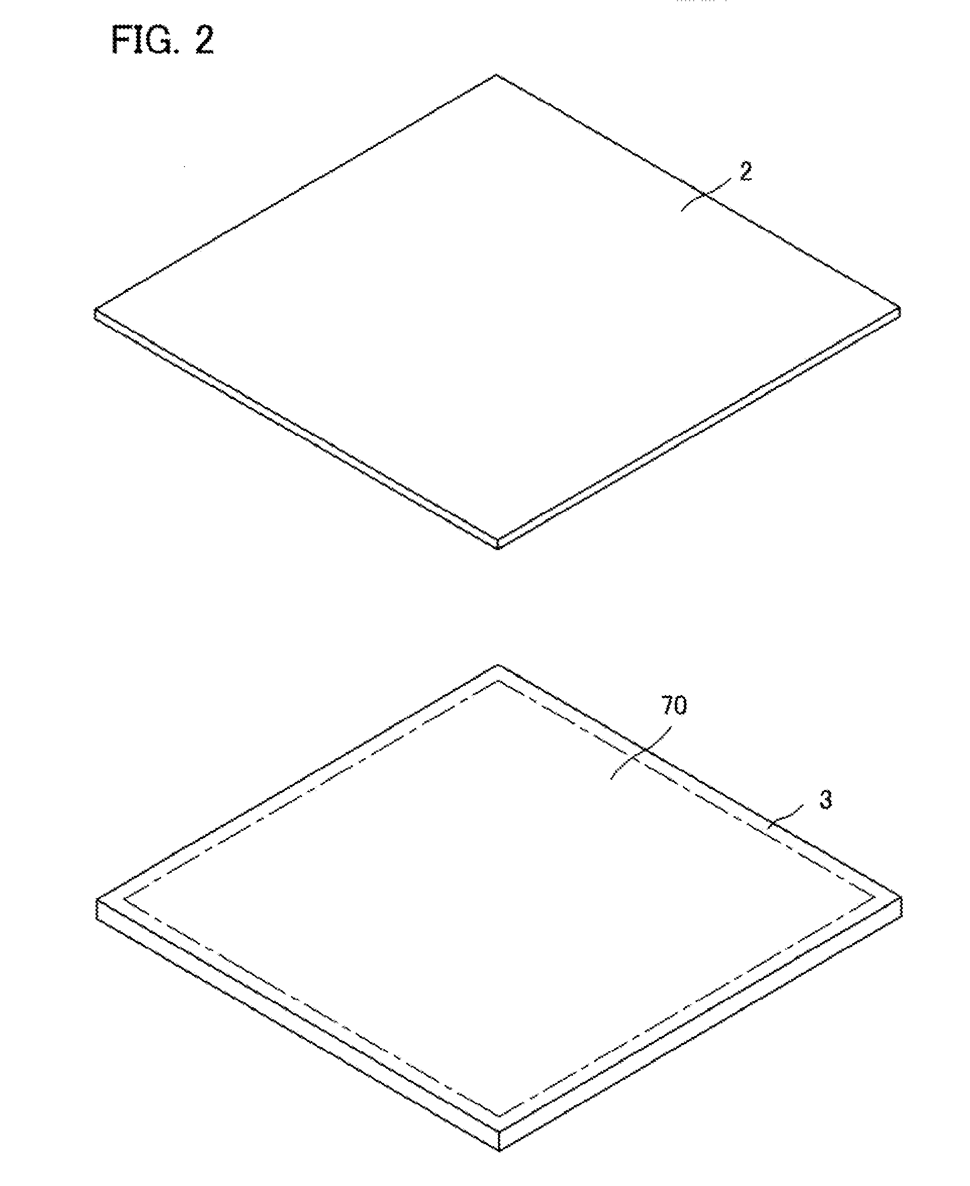
[0330]Next, a function of the displaying unit 1 of the first embodiment will be described.
[0331]In the displaying unit 1, the second insulating substrate 114 transmits a portion of irradiation light from the color filter 113 of the display device 3 and, the light reaches the second polarizing member 115. Then, only light in a certain vibration direction passes through the second polarizing member 115, is refracted by an interface between the second polarizing member 115 and the first substrate 15 of the touch panel 2, and is introduced into the touch panel 2.
[0332]When the side face part 32 (side face part 31) of the first wiring line 21 is upright with respect to the distal end face 33, the light is reflected by the side face part 32 (side face part 31) as illustrated in FIG. 15B. Thus, the light reflected by the side face part 32 travels to the user side, and the side face part 32 of the first wiring line 21 is visible from the user side, which may cause deterioration in appearanc...
second embodiment
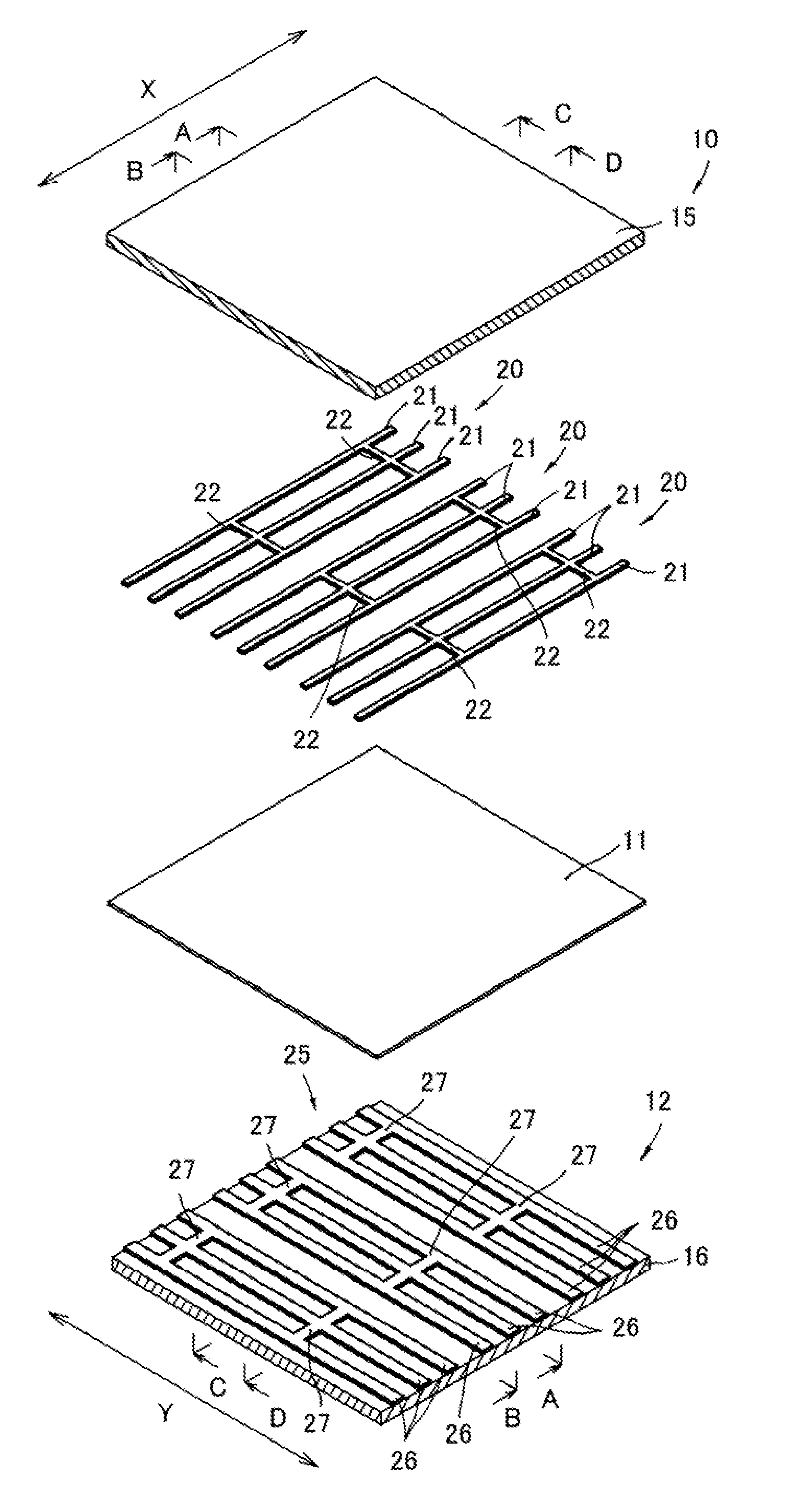
[0341]That is, in a touch panel 120 of the second embodiment, a first electrode group 20 and / or a second electrode group 25 is formed by a subtractive method.
[0342]Method for Manufacturing Touch Panel 120 by Using Subtractive Method
[0343]Hereinbelow, a method for manufacturing the touch panel 120 in the second embodiment will be described.
[0344]In a first electrode group forming step (electrode group forming step) of the second embodiment, a conductive layer forming step of forming a conductive layer 124 on a first substrate 15 is first performed.
[0345]Specifically, as illustrated in FIGS. 17A and 17B, a metal catalyst is applied to one face of the first substrate 15 to form a seed layer 80 (seed layer forming step).
[0346]Subsequently, as illustrated in FIG. 17C, a first plating layer 81 is formed by electroless plating on the first substrate 15 having the seed layer 80 formed thereon (first plating step).
[0347]Subsequently, as illustrated in FIG. 17D, a second plating layer 121 is ...
third embodiment
[0372]Specifically, patterning of respective electrode groups 20, 25 of a touch panel 150 of the third embodiment is performed by laser scribe.
[0373]Hereinbelow, the method for manufacturing the touch panel 150 of the third embodiment will be described. Note that since the method for manufacturing the touch panel 150 is the same as the method for manufacturing the touch panel 2 of the first embodiment except for a first electrode group forming step of forming the first electrode group 20 and a second electrode group forming step of forming the second electrode group 25, description of the same steps will be omitted.
[0374]Method for Manufacturing Touch Panel 2 by Using Laser Generator
[0375]First, in the first electrode group forming step (electrode group forming step) of the third embodiment, as illustrated in FIGS. 20A and 20B, a conductive layer 151 is formed on a first substrate 15 (conductive layer forming step).
[0376]A method for forming the conductive layer 151 at this time is ...
PUM
 Abstract
Description
Claims
Application Information


