Electromagnetic wave shielding filter and process for producing the same
a technology electromagnetic shielding filter, which is applied in the direction of superimposed coating process, cathode ray tube/electron beam tube, coating, etc., can solve the problem of electromagnetic shielding filter having insufficient electromagnetic shielding ability, white dispersed image, low invisibility of the mesh, etc. problem, to achieve the effect of good adhesion, small number of steps, and short tim
- Summary
- Abstract
- Description
- Claims
- Application Information
AI Technical Summary
Benefits of technology
Problems solved by technology
Method used
Image
Examples
modified embodiment
[0091]The present invention encompasses the following modification.
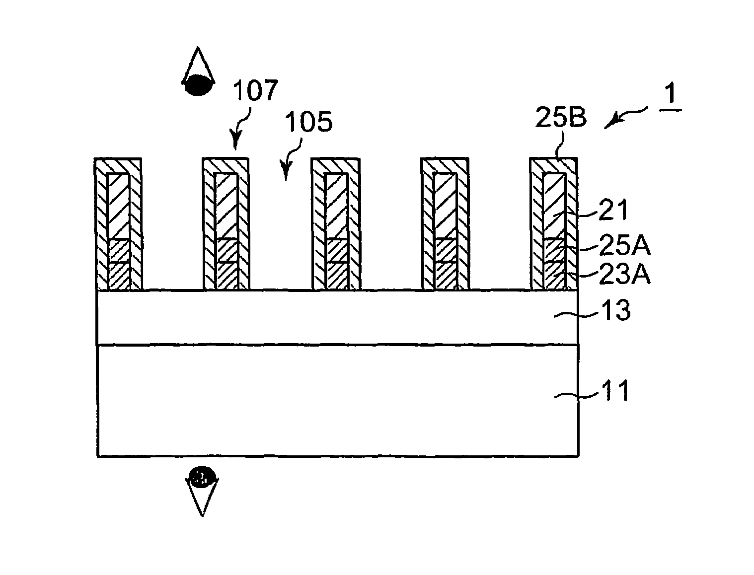
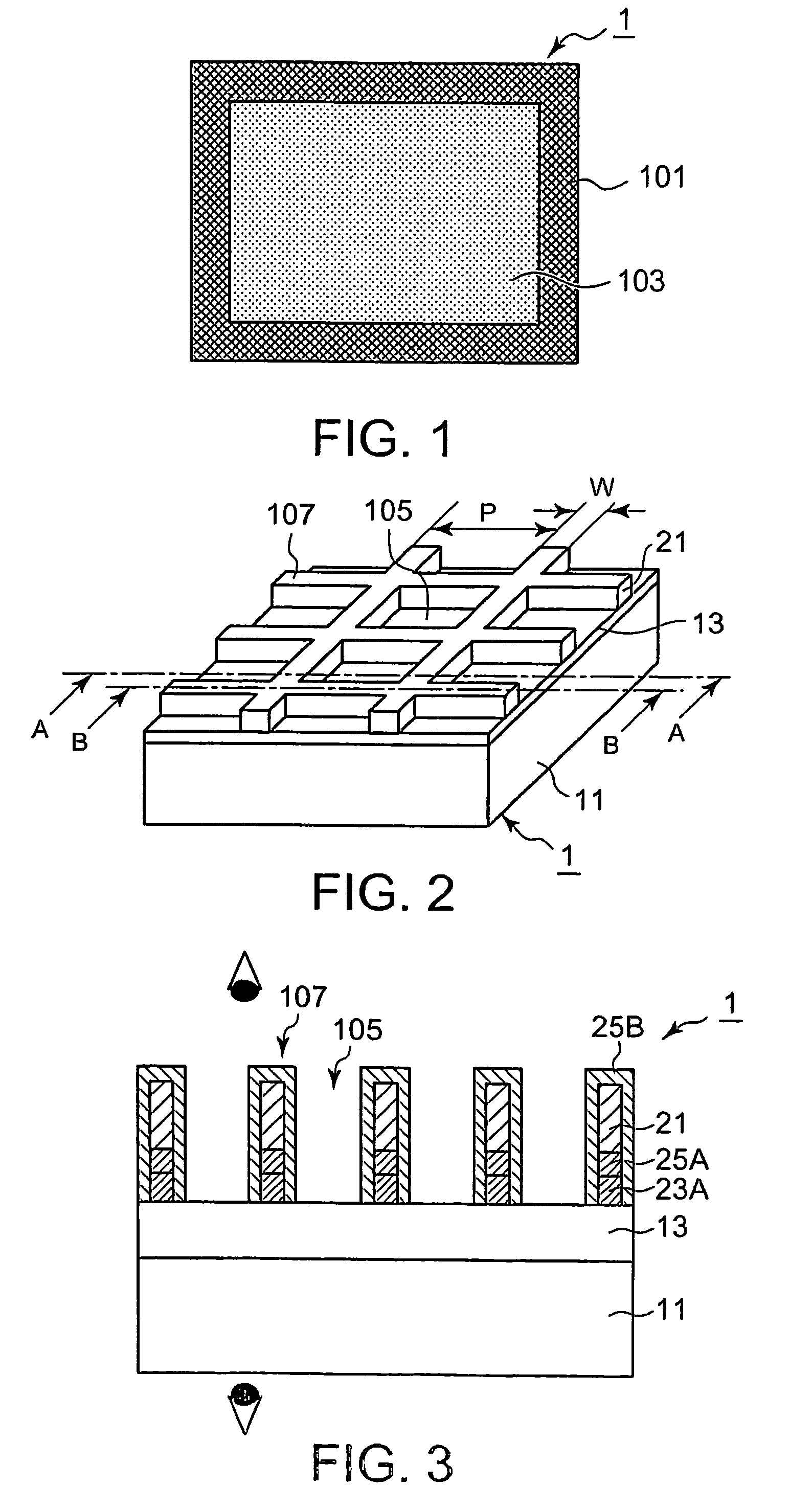
[0092]After obtaining the electromagnetic wave shielding filter 1 shown in FIG. 3, the surface of the mesh part 103 that is rough due to the line parts 107 and the openings 105 may be smoothened by filling the openings 105 with a transparent resin. If the surface of the mesh part 103 is smoothened in this manner, air bubbles never remain in the openings 105 when the mesh part of the electromagnetic wave shielding filter and another member (a transparent substrate, a near infrared ray absorbing filter, an antireflection filter, or the like) are laminated with an adhesive layer in the later step. It is thus possible to avoid lowering of the sharpness of a displayed image that occurs if air bubbles remain in the openings and scatter light.
example 1
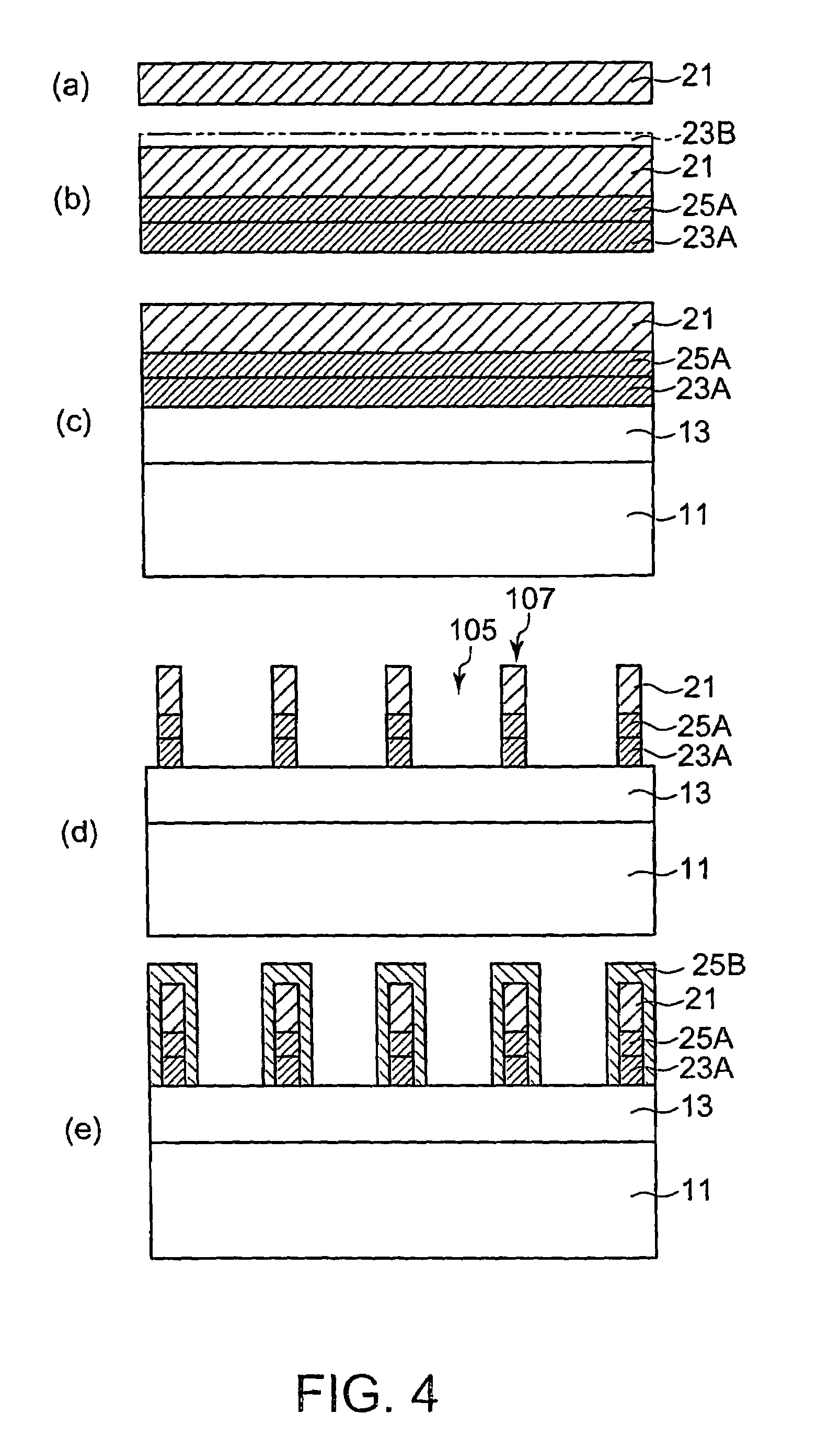
[0094]Electrolytic copper foil with a thickness of 10 μm was used as the metal layer 21. Copper-cobalt alloy particles (mean particle diameter: 0.3 μm) were cathodically electrodeposited on one surface of the metal layer 21, thereby forming a first blackening layer 25A. After effecting zinc plating, conventional chromate treatment was conducted by dipping to make both surfaces of the metal layer 21 anticorrosive. The anticorrosive layer present on the first blackening layer 25A surface is herein referred to as an anticorrosive layer 23A, and the anticorrosive layer present on the metal layer surface, a second anticorrosive layer 23B.
[0095]The anticorrosive layer 23A on the side of the first blackening layer 25A and a transparent substrate 11 made of a PET film A4300 (trademark of a polyethylene terephthalate film, manufactured by Toyobo Co., Ltd., Japan) with a thickness of 100 μm were laminated with an adhesive layer 13 of a two-part curing urethane adhesive, and this laminate was ...
example 2
[0099]An electromagnetic wave shielding filter 1 was obtained in the same manner as in Example 1, except that electroplating was conducted by immersing the laminate in an aqueous solution mixture of an aqueous ammonium solution of nickel sulfate, an aqueous solution of tin sulfate and an aqueous solution of sodium thiosulfate, serving as a plating bath for blackening treatment, thereby depositing a nickel-tin alloy as the second blackening layer 25B.
PUM
| Property | Measurement | Unit |
|---|---|---|
| frequency | aaaaa | aaaaa |
| thickness | aaaaa | aaaaa |
| thickness | aaaaa | aaaaa |
Abstract
Description
Claims
Application Information


