Data property-based data placement in a nonvolatile memory device

Active Publication Date: 2017-01-19
SAMSUNG ELECTRONICS CO LTD
View PDF83 Cites 44 Cited by
  • Summary
  • Abstract
  • Description
  • Claims
  • Application Information

AI Technical Summary

Benefits of technology

The patent describes a method for data placement in a nonvolatile memory device based on data property identifiers. The method involves detecting an executing application or hardware device, searching a workflow repository to find a predetermined workflow associated with the application or hardware device, comparing the activities of the application or hardware device to the workflow, and automatically assigning data property identifiers to data items based on the comparison. This allows for efficient placement of data in the nonvolatile memory device. The patent also includes a system for data property-based data placement and a computer program for executing the method.

Problems solved by technology

Since the NAND flash storage cells in SSDs have very unique properties, SSD's normal usages are very inefficient.
Thus, garbage collection overhead is one of the biggest speed limiters in the technology class, incurring higher data I / O latency and lower I / O performance.
Therefore, operating systems (OS) and applications, which don't treat hot / cold data differently, and store them together, will see performance degradation over time (compared to OS's and applications that do treat hot and cold data differently), as well as a shorter SSD lifetime as more erase cycles are needed, causing the NAND cells to wear out faster.
However, to utilize this new interface, many changes within the applications (including source code) and the OS are required.
As a typical computer can have tens or hundreds of software applications installed and running, it's very difficult for all applications, especially for legacy and closed-source applications, to adapt to those changes, in order to use SSDs more efficiently.
In addition, multi-stream SSD has limited applicability in that multi-stream SSD is only compatible for use by operating systems and applications that now how to use it.

Method used


Image

  • Data property-based data placement in a nonvolatile memory device
  • Data property-based data placement in a nonvolatile memory device
  • Data property-based data placement in a nonvolatile memory device

Examples


Embodiment Construction

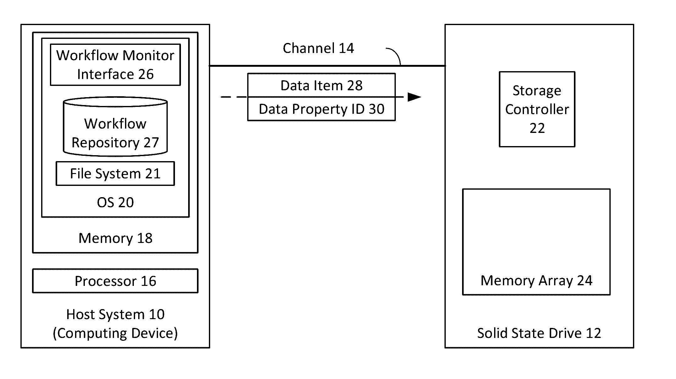
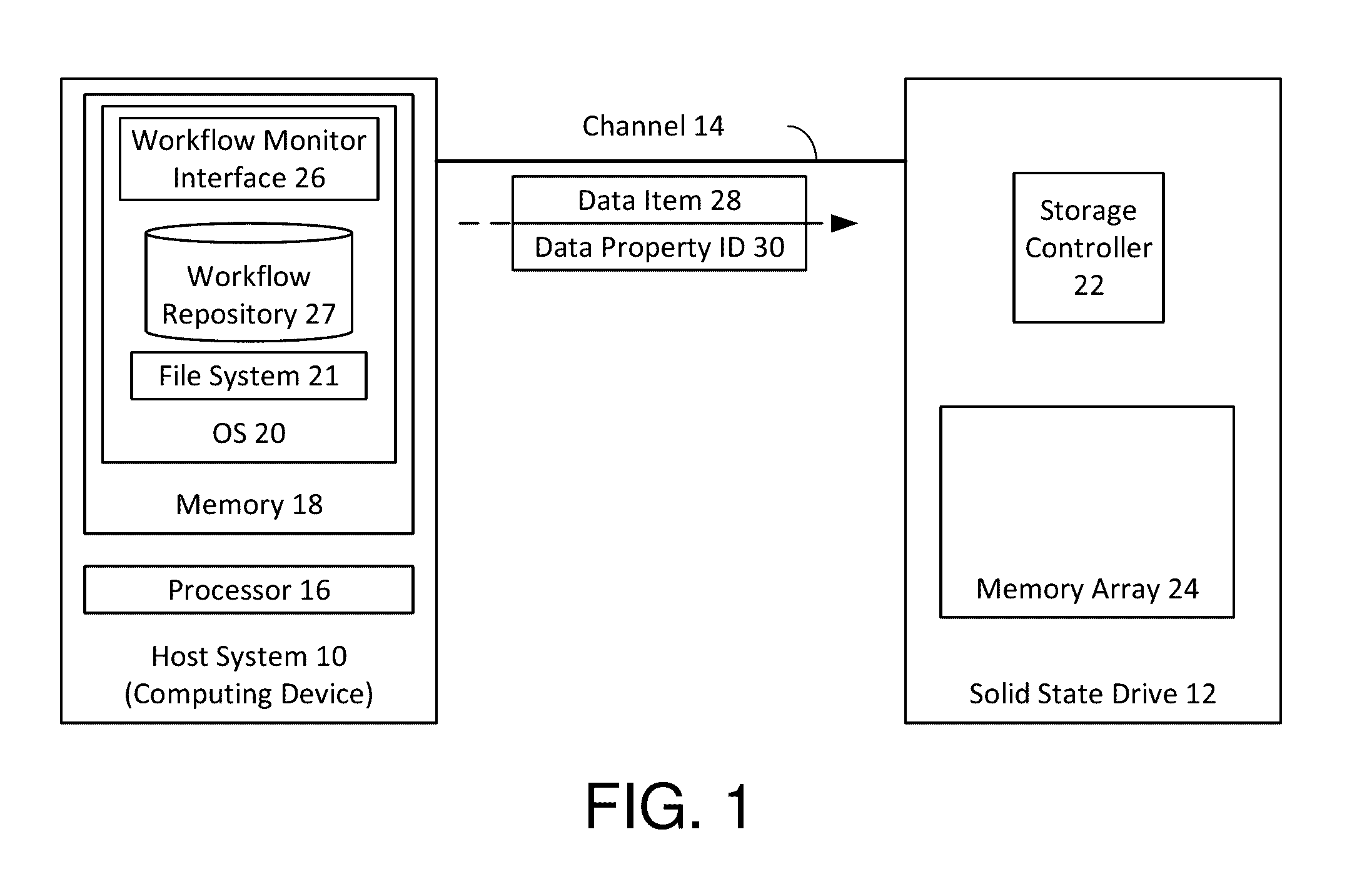
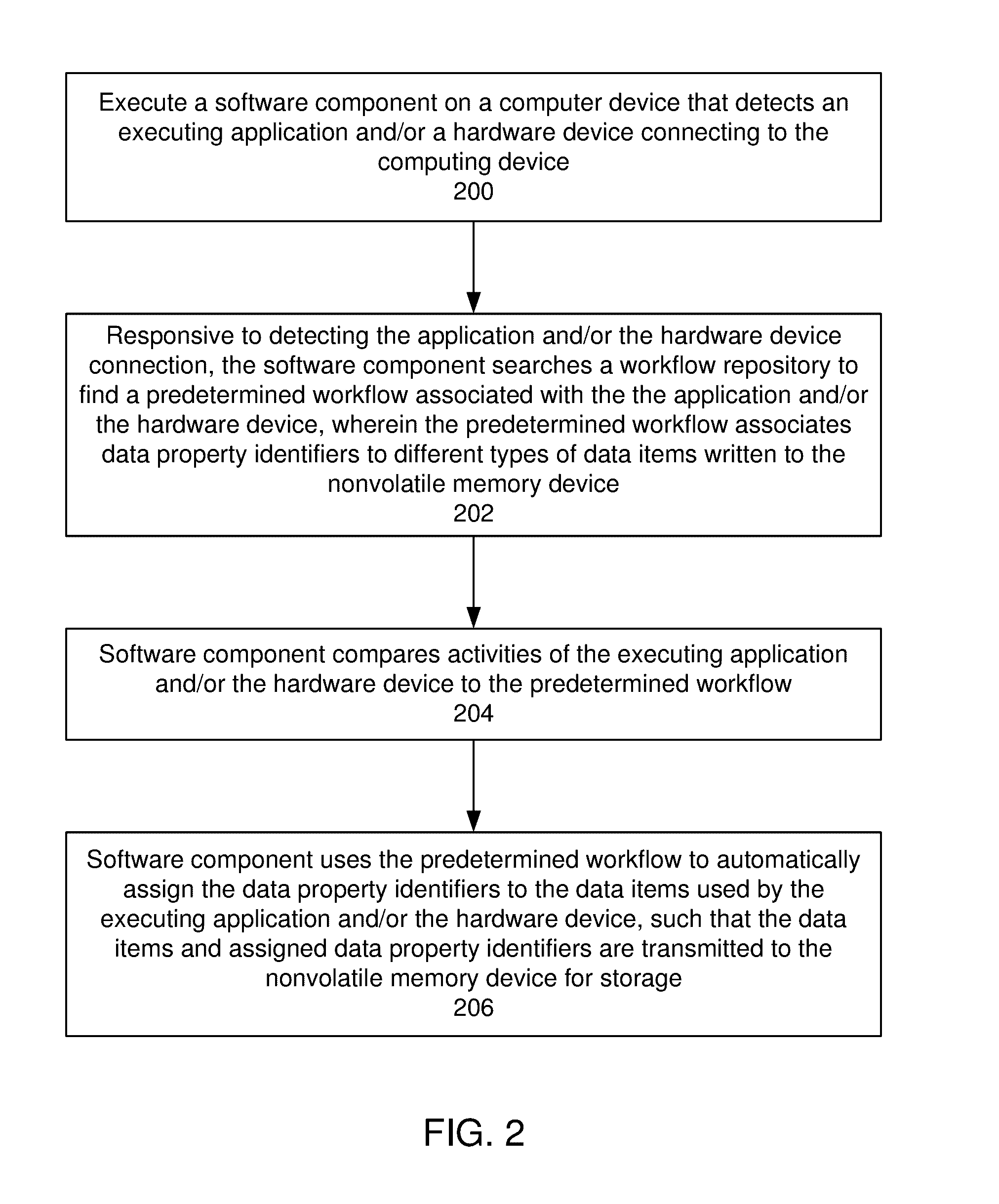
[0022]Reference will now be made in detail to the embodiments of the present general inventive concept, examples of which are illustrated in the accompanying drawings, wherein like reference numerals refer to the like elements throughout. The embodiments are described below in order to explain the present general inventive concept while referring to the figures.

[0023]Advantages and features of the present invention and methods of accomplishing the same may be understood more readily by reference to the following detailed description of embodiments and the accompanying drawings. The present general inventive concept may, however, be embodied in many different forms and should not be construed as being limited to the embodiments set forth herein. Rather, these embodiments are provided so that this disclosure will be thorough and complete and will fully convey the concept of the general inventive concept to those skilled in the art, and the present general inventive concept will only b...


PUM


Abstract

Example embodiments are described for data property-based data placement inside a nonvolatile memory device performed by a storage controller of the nonvolatile memory device. In one aspect, the embodiments include: executing a software component on the computer device that detects at least one of an executing application and a hardware device connecting to the computing device; responsive to detecting the at least one executing application and the hardware device, searching, by the software component, a workflow repository to find a predetermined workflow associated with the at least one executing application and the hardware device, wherein the predetermined workflow associates predefined data property identifiers to different types of data items written to the nonvolatile memory device by the executing application or the hardware device; comparing, by the software component, activities of the at least one executing application and the hardware device to the predetermined workflow; and using the predetermined workflow to automatically assign the data property identifiers to the data items used by the application or the hardware device, such that the data items and assigned data property identifiers are transmitted over a channel to the nonvolatile memory device for storage wherein the nonvolatile memory device reads the data property identifiers and identifies which blocks of the nonvolatile memory device to store the corresponding data items, such that the data items having the same data property identifiers are stored in a same block.

Description

CROSS-REFERENCE TO RELATED APPLICATIONS[0001]This application claims the benefit of provisional Patent Application Ser. No. 62 / 192,045, filed Jul. 13, 2015, and provisional Patent Application Ser. No. 62 / 245,100, filed Oct. 22, 2015, both incorporated herein by reference.BACKGROUND[0002]Flash memory based solid-state drives (SSD) have been used widely in both consumer computers and enterprise servers. There are two main types of flash memory, which are named after the NAND and NOR logic gates. NAND type flash memory may be written and read in blocks, each of which comprises a number of pages.[0003]Since the NAND flash storage cells in SSDs have very unique properties, SSD's normal usages are very inefficient. For example, although it can be randomly read or programmed a page at a time, NAND flash memory can only be erased a block at a time. To rewrite a single NAND Flash page, the whole erase block (which contains a lot of flash pages) has to be erased first.[0004]Since NAND flash b...

Claims


Application Information

Patent Timeline
IPC IPC(8): G06F3/06G06F12/02
CPCG06F3/0611G06F3/0688G06F2212/702G06F3/0653G06F12/0253G06F3/0647G06F3/0607G06F3/0616G06F3/064G06F3/0643G06F3/0679G06F12/0246G06F2212/1016G06F2212/7202G06F2212/7205G06F3/0689
Inventor CHOI, CHANGHOHUO, JIANJIANTSENG, DERRICKKRISHNAMOORTHY, PRAVEENHUEN, HINGKWAN
Owner SAMSUNG ELECTRONICS CO LTD
Why Eureka
Try Eureka