Lead frame, semiconductor device, method for manufacturing lead frame, and method for manufacturing semiconductor device

a semiconductor device and lead frame technology, applied in semiconductor devices, semiconductor/solid-state device details, electrical devices, etc., can solve the problems of reduced heat dissipation and large package size of semiconductor devices, and achieve the effect of reducing the occurrence of solder cracks

Active Publication Date: 2017-01-26
SHINDENGEN ELECTRIC MFG CO LTD
View PDF2 Cites 24 Cited by
  • Summary
  • Abstract
  • Description
  • Claims
  • Application Information

AI Technical Summary

Benefits of technology

[0037]According to the present invention, an outer region of the terminal portion of the lead is provided with a solder thickness ensuring portion where the facing surface, which faces conductive patterns on the wiring board, is depressed toward the back surface in the terminal portion. The solder thickness ensuring portion is thinner than a center region of the facing surface in the terminal portion. A center region of the back surface is flat without a depression. This ensures a solder thickness for joining the terminal portion of the lead and the wiring board together in the outer region of the terminal portion where stress tends to concentrate, and thereby reduces the occurrence of solder crack, due to a temperature change, even with the use of a mold resin with a low coefficient of linear expansion as a resin for encapsulation of the semiconductor device.

Problems solved by technology

Such a semiconductor device, however, has a larger package size than a discrete device, such as a switching device.
If the package warps due to a temperature change, the contact area between the wiring board and the heatsink decreases, resulting in lower heat dissipation.

Method used


Image

  • Lead frame, semiconductor device, method for manufacturing lead frame, and method for manufacturing semiconductor device
  • Lead frame, semiconductor device, method for manufacturing lead frame, and method for manufacturing semiconductor device
  • Lead frame, semiconductor device, method for manufacturing lead frame, and method for manufacturing semiconductor device

Examples


Embodiment Construction

[0049]One embodiment of the present invention will now be described with reference to the attached drawings. Components having the same function are denoted by the same reference sign throughout the drawings and detailed description of the components with the same reference sign will not be repeated.

Lead Frame

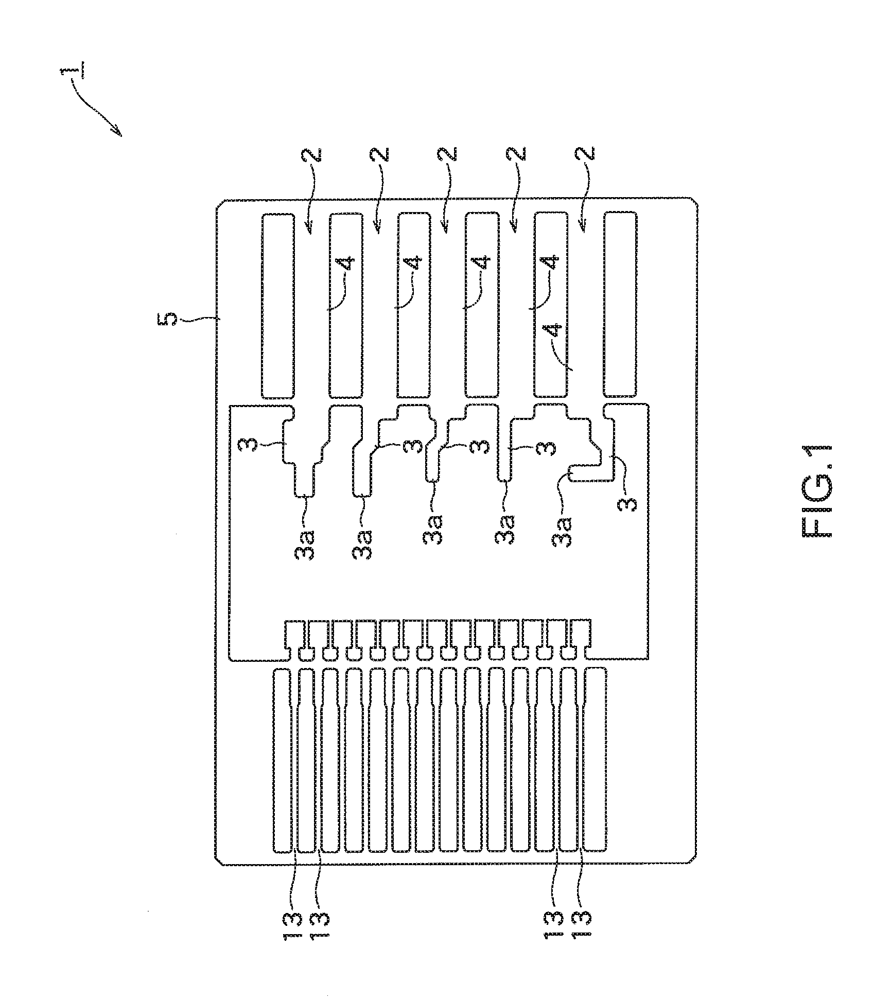
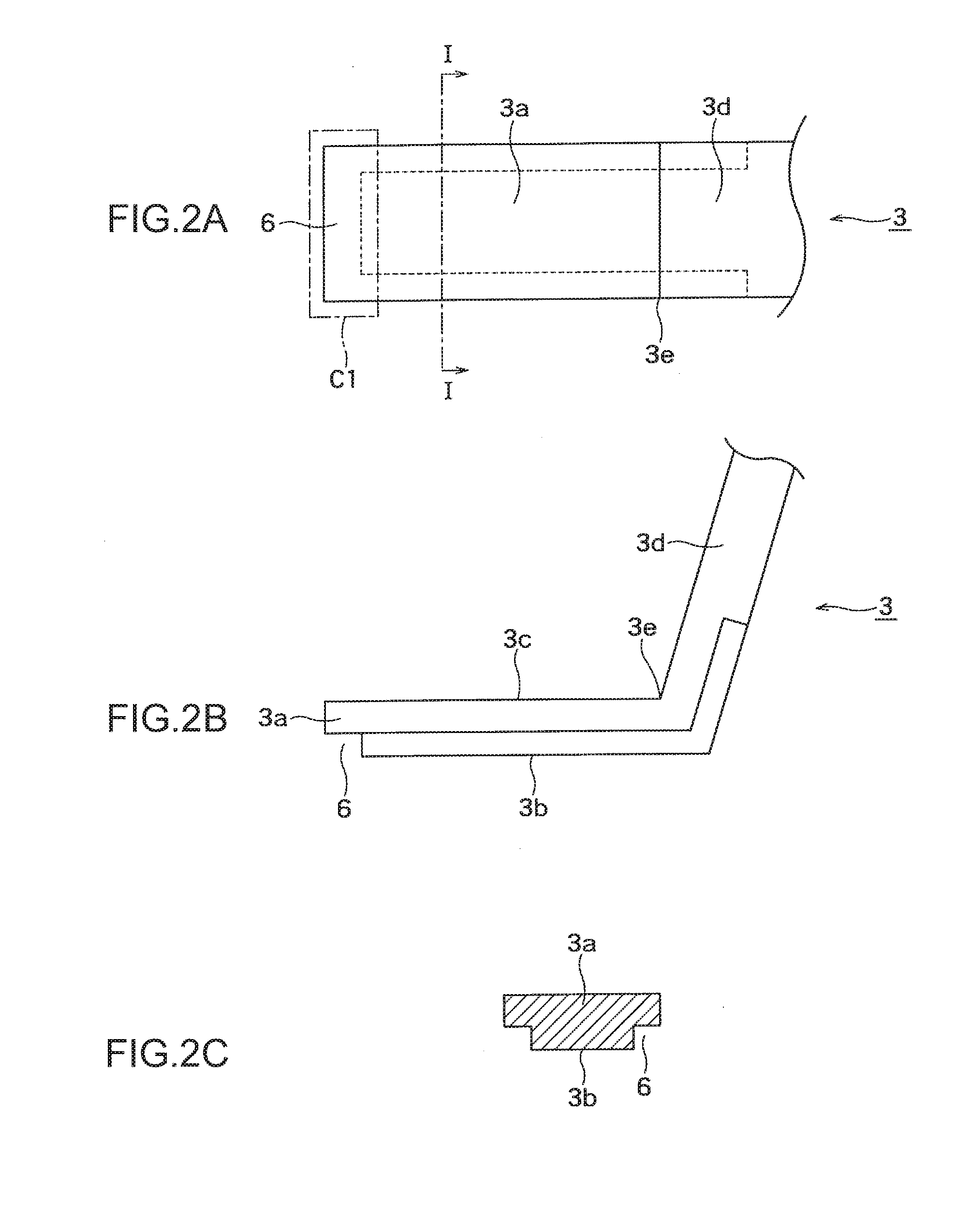
[0050]First, a lead frame 1 according to the embodiment of the present invention will be described with reference to FIGS. 1, 2A, 2B and 2C.

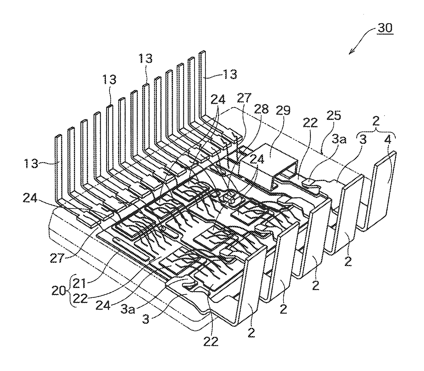
[0051]As illustrated in FIG. 1, the lead frame 1 includes a plurality of lead parts 2 and a frame unit 5 supporting the plurality of lead parts 2. Each lead part 2 includes an inner lead 3 and an outer lead 4 connected to the inner lead 3. As illustrated in FIG. 1, the lead frame 1 further includes a plurality of lead parts 13 facing the lead parts 2. When the lead frame 1 is used for a semiconductor device of a switching power supply, for example, the lead parts 2 serve as a power supply terminal, a ground terminal, a current output termin...


PUM


Abstract

A lead frame according to one embodiment includes a lead part including an inner lead and an outer lead connected to the inner lead, and a frame unit supporting the lead part. The inner lead has a terminal portion having a facing surface and a back surface in the opposite side from the facing surface. The facing surface faces a conductive pattern of a wiring board. An outer region of the terminal portion is provided with a solder thickness ensuring portion where the facing surface is depressed toward the back surface
The solder thickness ensuring portion is thinner than a center region of the facing surface. A center region of the back surface is flat without a depression.

Description

TECHNICAL FIELD[0001]The present invention relates to a lead frame, a semiconductor device, a method for manufacturing the lead frame, and a method for manufacturing the semiconductor device.BACKGROUND ART[0002]Semiconductor devices have been known which are fabricated by soldering metal leads and conductive patterns on a wiring board together, and then encapsulating the leads (inner leads), the mounting surface of the wiring board, and the electronic components mounted on the wiring board with a mold resin. To increase heat dissipation, some of these semiconductor devices are provided with a heatsink on the exposed surface uncovered with the mold resin, which is the opposite side of the wiring board from the mounting surface.[0003]Such a semiconductor device, however, has a larger package size than a discrete device, such as a switching device. If the package warps due to a temperature change, the contact area between the wiring board and the heatsink decreases, resulting in lower ...

Claims


Application Information

Patent Timeline
Patent Type & Authority Applications(United States)
IPC IPC(8): H01L23/495H01L21/48
CPCH01L23/49551H01L21/4842H01L23/49548H01L2224/48091H01L2224/48472H01L2224/49111H01L2924/0002H01L23/3735H01L23/49531H01L23/49562H01L23/49575H01L23/49582H01L23/49811H01L2924/00014H01L23/62H01L2924/00
Inventor KAMIYAMA, YOSHIHIROUMEDA, SOICHIRO
Owner SHINDENGEN ELECTRIC MFG CO LTD
Why Eureka
Try Eureka