Multichip module, on board computer, sensor interface substrate, and the multichip module manufacturing method

a multi-chip module and sensor interface technology, applied in the direction of electrical equipment, semiconductor devices, semiconductor/solid-state device details, etc., can solve the problems of difficult downsizing and lightening of mcm b>101/b>, and achieve high-density mounting, improve yield, and maintain performance

Active Publication Date: 2017-01-26
MITSUBISHI HEAVY IND LTD
View PDF6 Cites 9 Cited by
  • Summary
  • Abstract
  • Description
  • Claims
  • Application Information

AI Technical Summary

Benefits of technology

[0015]In such a multichip module manufacturing method, the plurality of semiconductor substrates are stacked by the room-temperature bonding method. Therefore, a heat load is never applied to a surface mounting part upon stacking. Therefore, there is no fear that a surface mounting part is broken in an assembling step, and the yield is improved. Also, the manufactured multichip module has the above-mentioned configuration and can realize downsizing, lightening and high-density mounting and so on.
[0016]By the present invention, it is possible to provide the multichip module, the on board computer and the multichip module manufacturing method, in which the downsizing and the lightening are possible while maintaining a performance. Also, it is possible to provide the multichip module, the on board computer and the multichip module manufacturing method, in which there is no limitation of the number of layers theoretically while maintaining a performance.

Problems solved by technology

For this reason, it is difficult that the downsizing and lightening of the MCM 101 are dealt with.

Method used


Image

  • Multichip module, on board computer, sensor interface substrate, and the multichip module manufacturing method
  • Multichip module, on board computer, sensor interface substrate, and the multichip module manufacturing method
  • Multichip module, on board computer, sensor interface substrate, and the multichip module manufacturing method

Examples


Embodiment Construction

[0058]Hereinafter, a multichip module, an on board computer and a multichip module manufacturing method according to embodiments of the present invention will be will be described with reference to the attached drawings.

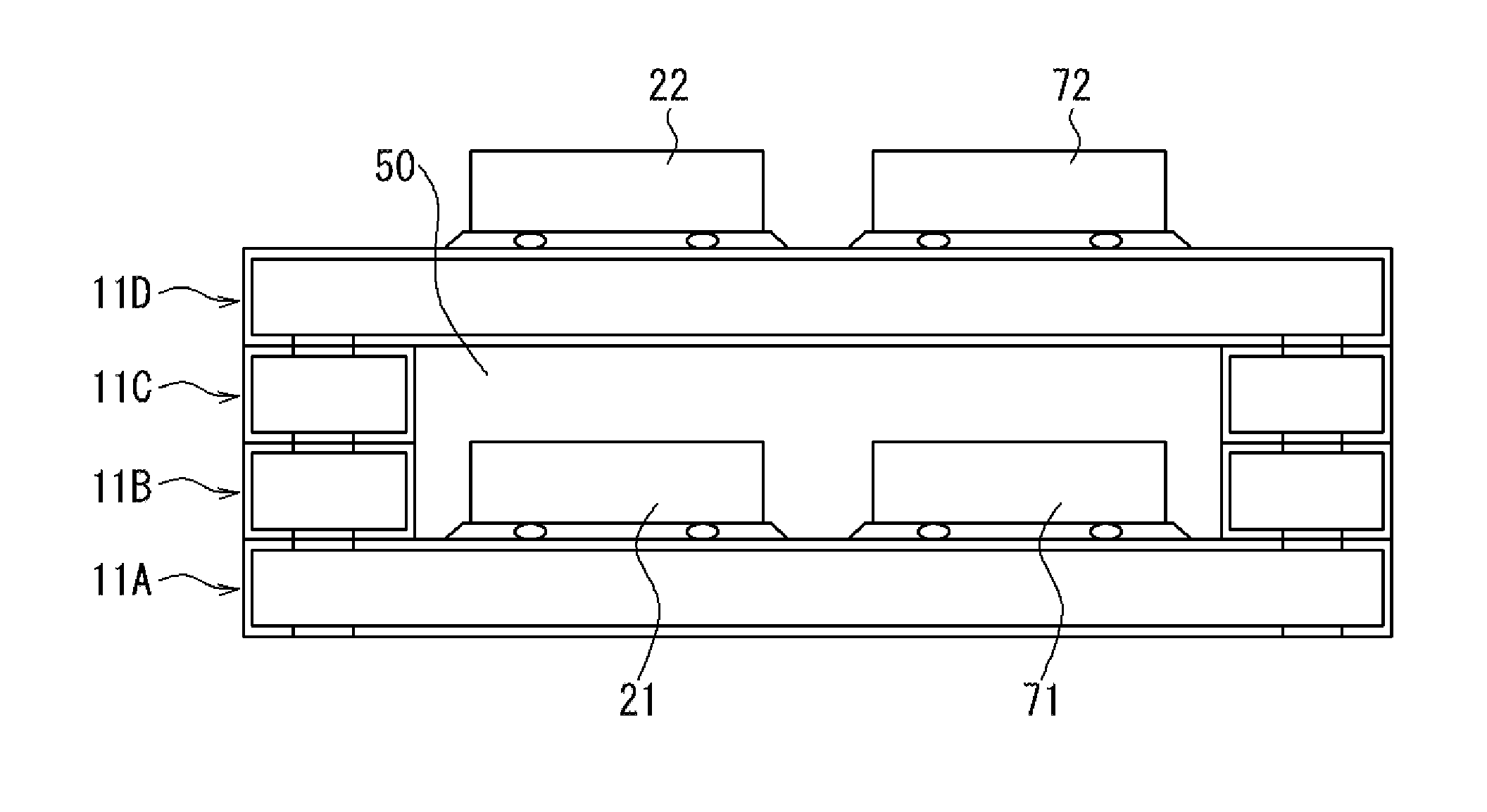
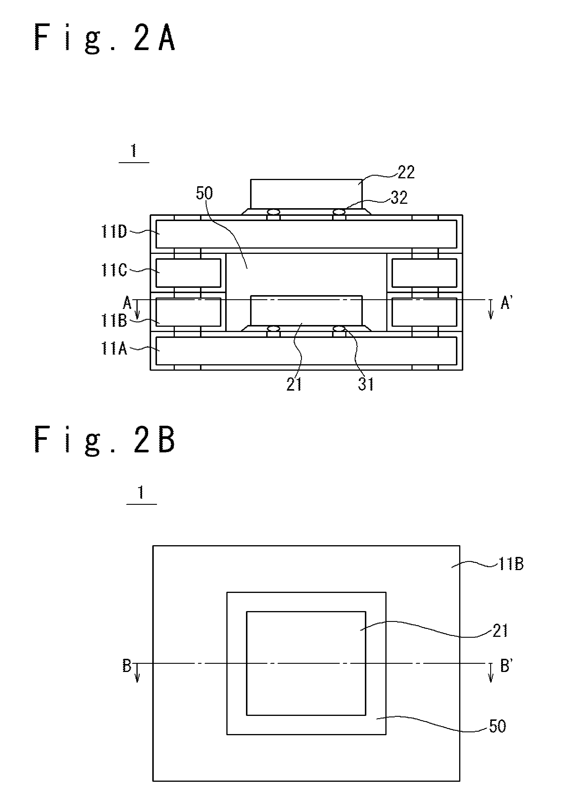
[0059]The configuration of the multichip module according to an embodiment will be described. FIG. 2A and FIG. 2B are sectional views schematically showing a configuration example of the multichip module according to the present embodiment. Here, FIG. 2A is the vertical sectional view along the BB′ line in FIG. 2B and FIG. 2B is the horizontal sectional view along the AA′ line in FIG. 2A. The multichip module 1 contains a plurality of semiconductor substrates 11A, 11B, 11C and 11D and a plurality of semiconductor chips 21 and 22 as a plurality of surface mounting parts (SMD).

[0060]Each of the plurality of semiconductor substrates 11A, 11B, 11C and 11D has a wiring line region which contains a wiring line passing through the substrate from one surface to the other sur...


PUM


Abstract

A multichip module includes a plurality of semiconductor substrates and a plurality of surface mounting parts. The plurality of semiconductor substrates each have a wiring line region which contains a wiring line to pierce from one of the surfaces to the other surface. A plurality of surface mounting parts are mounted on either of the plurality of surface mounting parts. The plurality of semiconductor substrates are stacked to form a multilayer structure. The first surface mounting part as at least one of the plurality of surface mounting parts is arranged in an inside region of the multilayer structure.

Description

TECHNICAL FIELD[0001]The present invention related to a multichip module, an on board computer and a multichip module manufacturing method. Especially, the present invention relates to a multichip module, an on board computer, a sensor interface substrate and a multichip module manufacturing method, which are for an electronic equipment in which downsizing and lightening are required.BACKGROUND ART[0002]The downsizing and lightening of the electronic equipment are requested. Especially, in a small satellite, it is strongly required to achieve high functionality, high performance, downsizing and lightening of a satellite while maintaining the size of the satellite. Therefore, it is necessary to further carry out downsizing and high density mounting even in an electronic device such as an information processing apparatus mounted in the satellite. It is possible to cope with the downsizing of the information processing apparatus to an extent by the technique such as SOC (System On Chip...

Claims


Application Information

Patent Timeline
Patent Type & Authority Applications(United States)
IPC IPC(8): H01L25/065H01L25/00H01L23/48
CPCH01L25/0657H01L23/481H01L25/0652H01L2225/06572H01L2225/06541H01L2225/06517H01L25/50H01L2224/16225H01L2224/32225H01L2224/73204H01L2924/15311H01L25/0655H01L23/49827H01L23/13H01L23/147H01L23/49822H01L23/49833H01L21/4857H01L2924/00
Inventor KATO, MASAHIROKURODA, YOSHIKATSU
Owner MITSUBISHI HEAVY IND LTD
Why Eureka
Try Eureka