Mask and method for manufacturing display panel

a technology for display panels and masks, applied in the field of masks and a manufacturing method of display panels, can solve the problems of pixel color mixing, color mixing, affecting the yield of oled products, etc., and achieve the effect of improving the resolution of the display panel and reducing the color mixing of the display panel

Inactive Publication Date: 2017-01-26
EVERDISPLAY OPTRONICS (SHANGHAI) CO LTD
View PDF2 Cites 9 Cited by
  • Summary
  • Abstract
  • Description
  • Claims
  • Application Information

AI Technical Summary

Benefits of technology

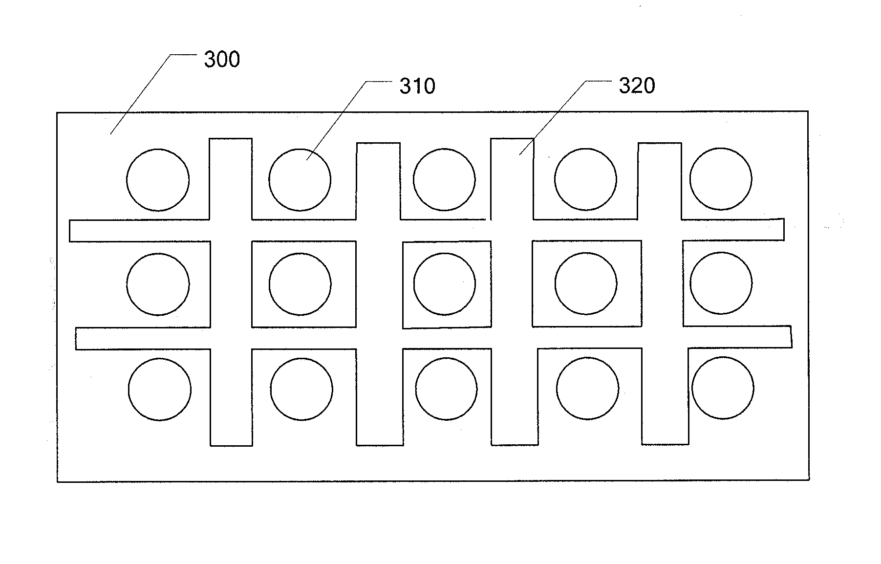
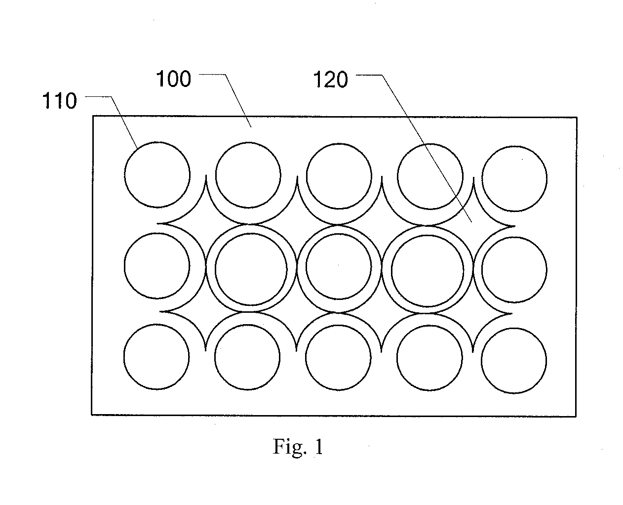
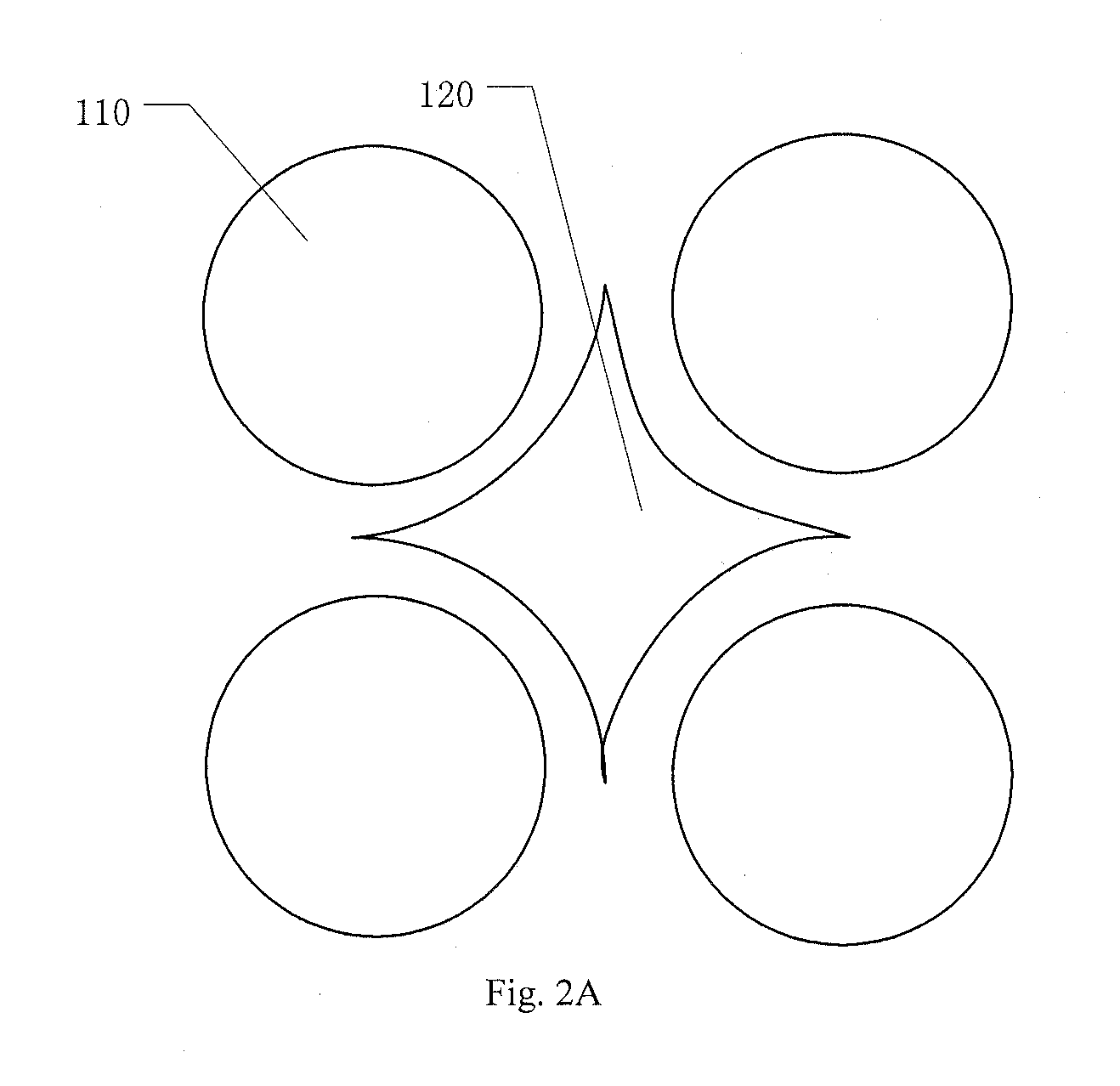
[0027]In the embodiments of the present disclosure, at least one partition member for separating thin film patterns which are to be formed according to openings in a mask is formed on the mask. Thus, the present disclosure can avoid the problem that organic materials may deviate the desired positions and laterally diffuse to adjacent pixel areas, and thereby the color mixing of the display panel can be reduced. Further, because the mask has partition members for separating thin film patterns which are to be formed according to openings in the mask, the intervals between adjacent pixels of the same or different colors can be reduced to improve resolution of the display panel.

Problems solved by technology

During processing, such masks are inclined to be deformed, thereby resulting in pixel color mixing.
Color mixing is one of the defects which influence the yield of OLED products.
Specifically, after a mask is stretched, the mask is not fully attached and in parallel with the substrate or some local unevenness occurs, and thus during evaporation, organic materials may deviate the desired positions and laterally diffuse to adjacent pixel areas.
Further, with the increasing of resolution the display panels, the color mixing becomes more serious.

Method used


Image

  • Mask and method for manufacturing display panel
  • Mask and method for manufacturing display panel
  • Mask and method for manufacturing display panel

Examples


Embodiment Construction

[0041]Now, exemplary implementations will be described more comprehensively with reference to the accompanying drawings. However, the exemplary implementations may be carried out in various manners, and shall not be interpreted as being limited to the implementations set forth herein; instead, providing these implementations will make the present disclosure more comprehensive and complete and will fully convey the conception of the exemplary implementations to the ordinary skills in this art. Throughout the drawings, the like reference numbers refer to the same or the like structures, and repeated descriptions will be omitted.

[0042]The features, structures or characteristics described herein may be combined in one or more embodiments in any suitable manner. In the following descriptions, many specific details are provided to facilitate sufficient understanding of the embodiments of the present disclosure. However, one of ordinary skills in this art will appreciate that the technical...


PUM

PropertyMeasurementUnit
central angleaaaaaaaaaa
partition areasaaaaaaaaaa
thicknessaaaaaaaaaa

Abstract

The present disclosure relates to a mask and a method for manufacturing a display panel. The mask includes: a body provided with a plurality of openings for defining pixel patterns and partition areas each of which is located among adjacent openings; and at least partition member provided on the partition areas. Using the mask and manufacturing provided by the present disclosure, pixel color mixing can be reduced.

Description

CROSS-REFERENCE TO RELATED APPLICATIONS[0001]This application claims priority to Chinese Patent Application No. 201510439851.0, filed Jul. 24, 2015, the entire contents of which are incorporated herein by reference.TECHNICAL FIELD[0002]The present disclosure generally relates to display technologies, and more particularly to a mask and a method for manufacturing a display panel.BACKGROUND[0003]Recently, with rapid development, Organic Light Emitting Diode (OLED) technology has become the most promising technology which may replace Liquid Crystal Displays (LCDs).[0004]When manufacturing an OLED substrate, respective layers in the organic light emitting device are formed by evaporation. Generally, masks having openings corresponding to thin film patterns to be formed are used to form thin film patterns corresponding to pixels on the substrate. In order to form the openings corresponding to the fine thin film patterns, masks usually have a very small thickness, and intervals between op...

Claims


Application Information

Patent Timeline
Patent Type & Authority Applications(United States)
IPC IPC(8): H01L51/00H01L27/32B05B15/04H01L51/56
CPCH01L51/0011H01L51/56H01L51/001H01L51/5012H01L27/3283B05B15/045H01L27/3246C23C14/042B05B12/20H10K59/12H10K71/166
Inventor HUANG, CHUN-CHIEH
Owner EVERDISPLAY OPTRONICS (SHANGHAI) CO LTD
Why Eureka
Try Eureka