Display device having reduced scan signal delay and driving method therefor

a technology of scan signal and display device, which is applied in the direction of instruments, static indicating devices, etc., can solve the problems of increasing the response time of scan lines, slow response speed of display devices, and increasing the response speed of scan signals, so as to reduce the response delay

Inactive Publication Date: 2017-02-16
SAMSUNG DISPLAY CO LTD
View PDF5 Cites 11 Cited by
  • Summary
  • Abstract
  • Description
  • Claims
  • Application Information

AI Technical Summary

Benefits of technology

[0010]Embodiments of the present invention provide a display device capable of reducing a response delay for a scan signal, as well as a corresponding driving method.
[0011]In addition, embodiments of the present invention provide a method for reducing a total RC for a charge rate of 99% while maintaining the same metal thickness.
[0012]Further, embodiments of the present invention provide a method for reducing a thickness of a scan line, and provide a display device without image quality deterioration associated with a voltage change of a data line, as well as associated driving methods.

Problems solved by technology

However, display devices having the structure as described above may exhibit slow response speed, since the plurality of pixels are connected to the scan lines and thus a resistive component and a capacitive component generated by the pixels cause the response time of the scan lines to slowly increase.
The response speed for the scan signal is thus becoming a more critical issue over time.

Method used


Image

  • Display device having reduced scan signal delay and driving method therefor
  • Display device having reduced scan signal delay and driving method therefor
  • Display device having reduced scan signal delay and driving method therefor

Examples


Embodiment Construction

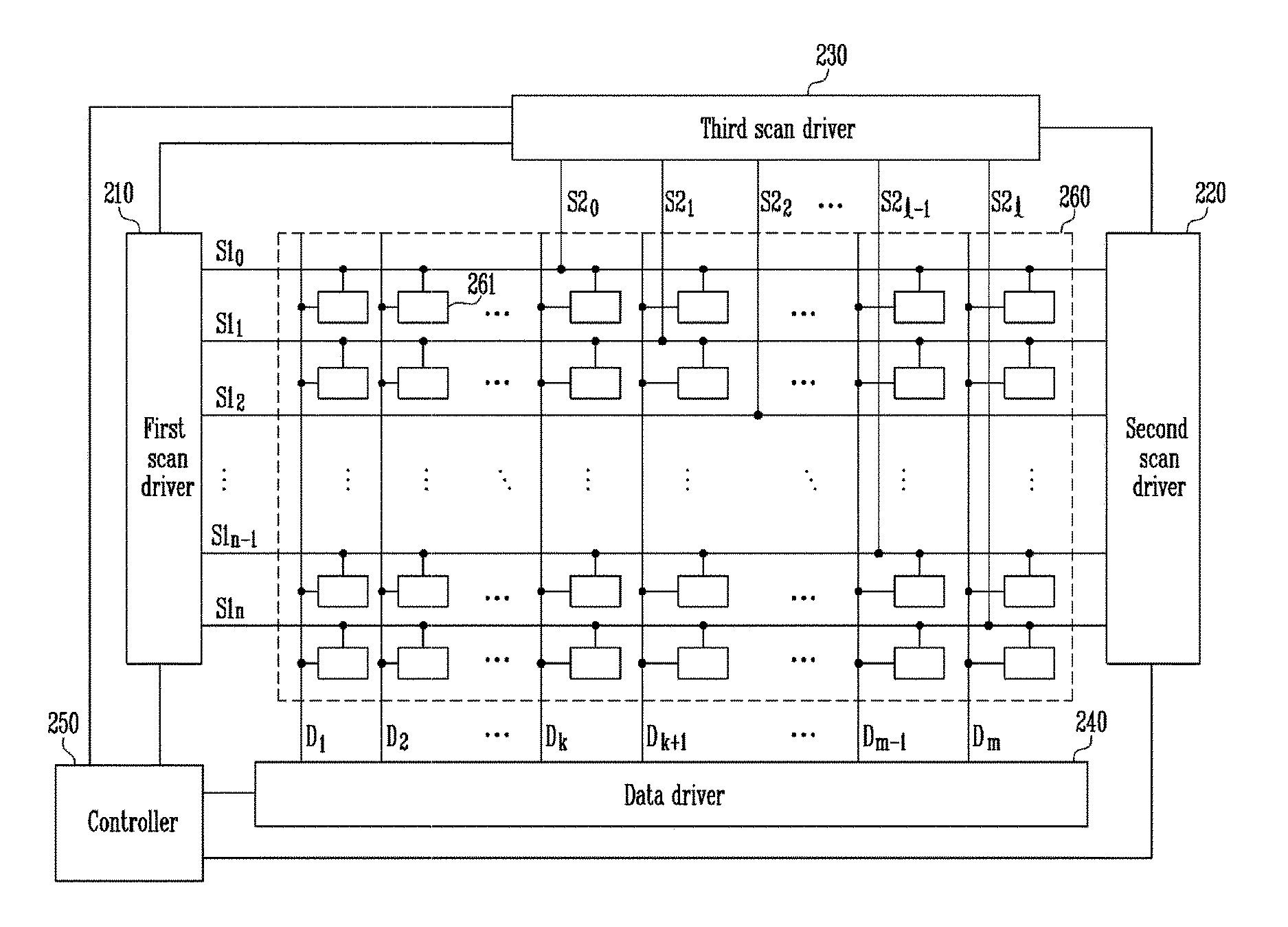
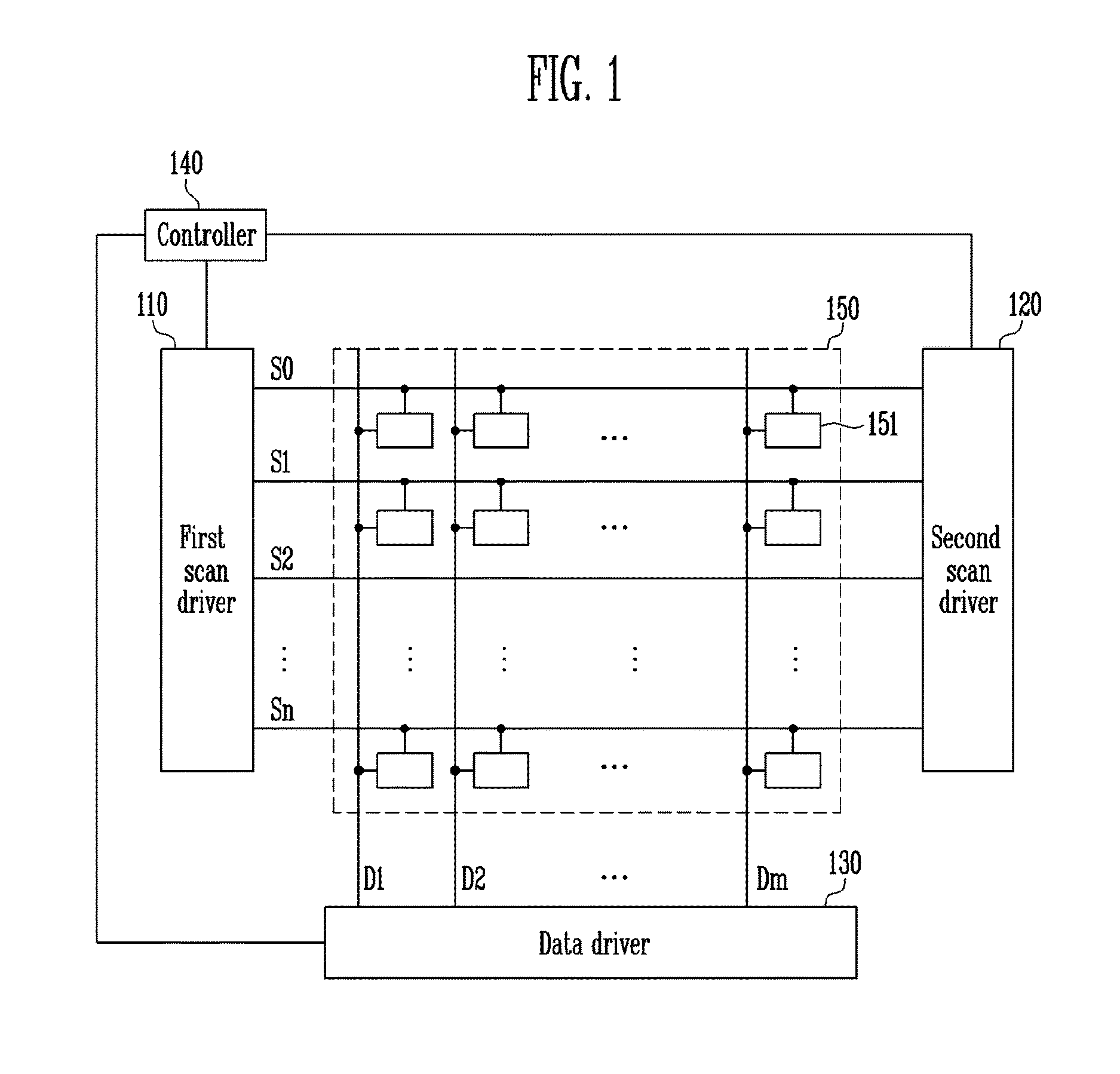
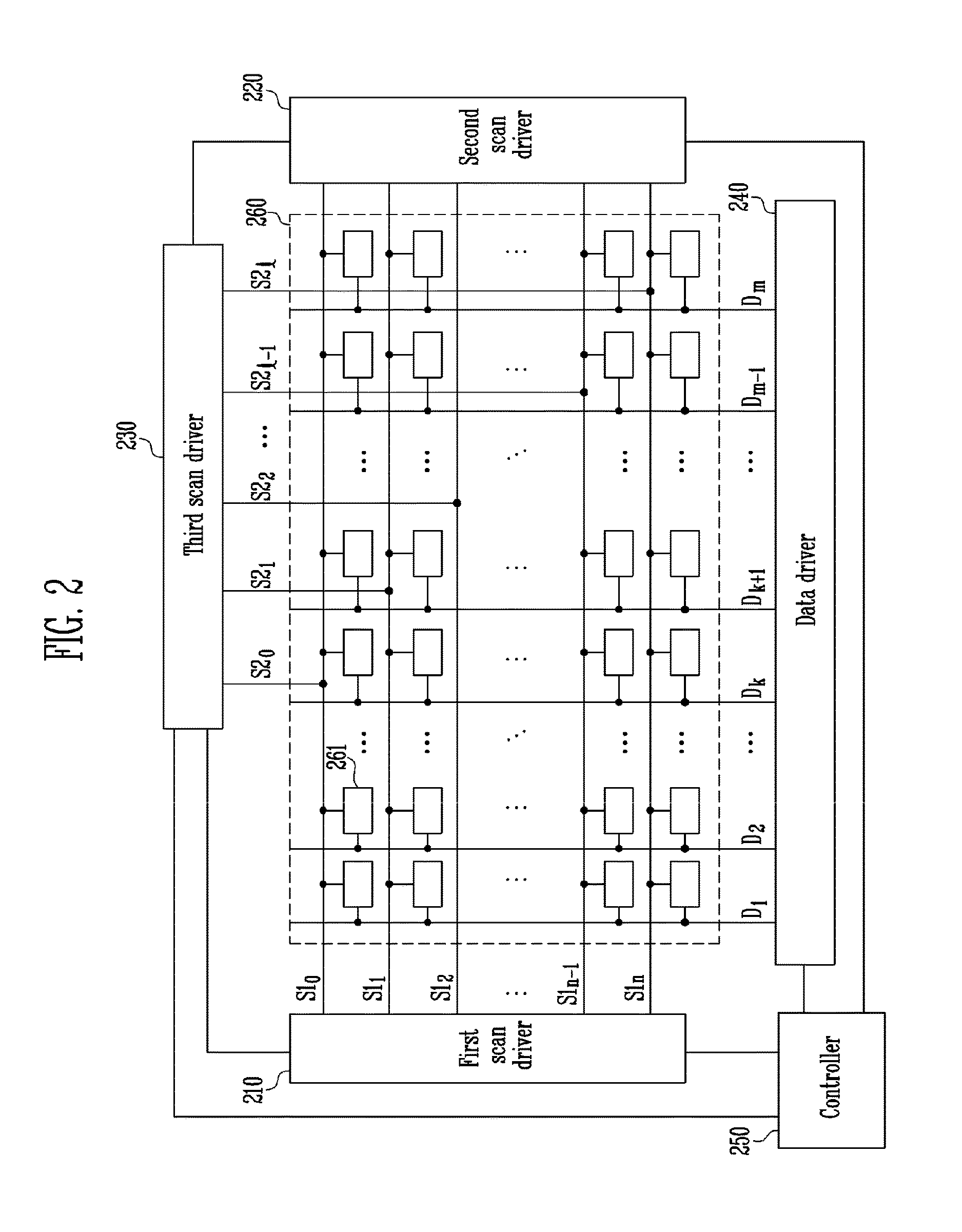
[0042]Hereinafter, exemplary embodiments of the present specification will be described in detail with reference to the attached drawings.

[0043]In describing exemplary embodiments, a description of technical details, which are well-known to technical fields to which the exemplary embodiment of the present specification belongs and which are not directly related to the exemplary embodiments of the present specification, will be omitted. This is to more clearly convey not obscure the subject matter of the present invention by eliminating the unnecessary description.

[0044]In the present specification, it is to be understood that when one component is referred to as being “connected” or “coupled” to another component, it may be connected or coupled directly to another component or be connected or coupled to another component with one or more other components intervening therebetween. In addition, unless explicitly described to the contrary, the word “comprise” or “comprising”, will be u...


PUM


Abstract

A display device according to an exemplary embodiment of the present invention may include: a display unit including a plurality of pixels; a first scan driver positioned at a first side of the display unit and arranged to output at least one first scan signal to the display unit; a second scan driver positioned at a second side of the display unit and arranged to output at least one second scan signal to the display unit; a third scan driver positioned along at least a portion of a third side of the display unit and arranged to output at least one third scan signal to the display unit; and a data driver positioned at a fourth side of the display unit and arranged to transmit a data signal to the display unit.

Description

CROSS-REFERENCE TO RELATED APPLICATION[0001]This application claims priority to, and the benefit of, Korean Patent Application No. 10-2015-0113897 filed on Aug. 12, 2015 in the Korean Intellectual Property Office, the entire contents of which are incorporated herein by reference in their entirety.BACKGROUND OF THE INVENTION[0002]1. Field[0003]Embodiments of the present invention relate generally to display devices. More specifically, embodiments of the present invention relate to display devices having reduced scan signal delay, and driving methods therefor.[0004]2. Description of the Related Art[0005]Display devices are required for computer monitors, televisions, mobile phones, and the like, and as such are currently widely used. Such display devices, which display an image using digital data, are classified into a cathode ray tube display device, a liquid crystal display (LCD), a plasma display panel (PDP), an organic light emitting diode (OLED) display, and the like. As display ...

Claims


Application Information

Patent Timeline
Patent Type & Authority Applications(United States)
IPC IPC(8): G09G3/20
CPCG09G2330/028G09G3/2092G09G2300/0426G09G2320/0223G09G2310/0281G09G2310/0267G09G3/3266
Inventor KIM, DONG GYULEE, JAE HOON
Owner SAMSUNG DISPLAY CO LTD
Why Eureka
Try Eureka