Display device

Active Publication Date: 2017-02-16
SHARP KK
View PDF0 Cites 4 Cited by
  • Summary
  • Abstract
  • Description
  • Claims
  • Application Information

AI Technical Summary

Benefits of technology

[0007]The display device according to an embodiment of the present invention

Problems solved by technology

Specifically, the planar display device is likely

Method used


Image

  • Display device
  • Display device
  • Display device

Examples


Example

First Embodiment

Liquid Crystal Display Device

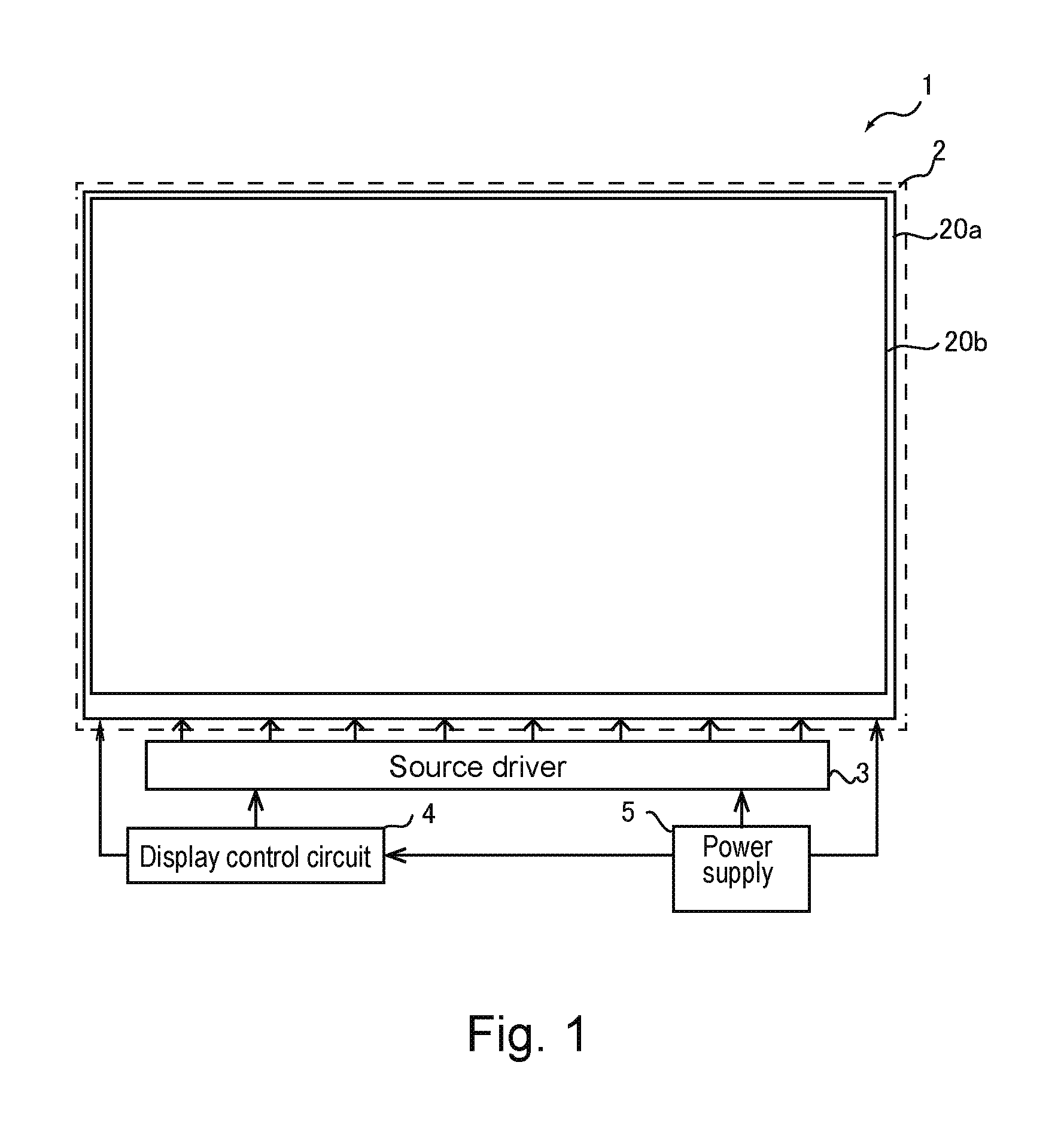
[0086]A liquid crystal display device 1 will now be described with reference to FIG. 1 as a display device according to the first embodiment of the present invention. FIG. 1 is a diagram depicting an outline configuration of the liquid crystal display device 1.

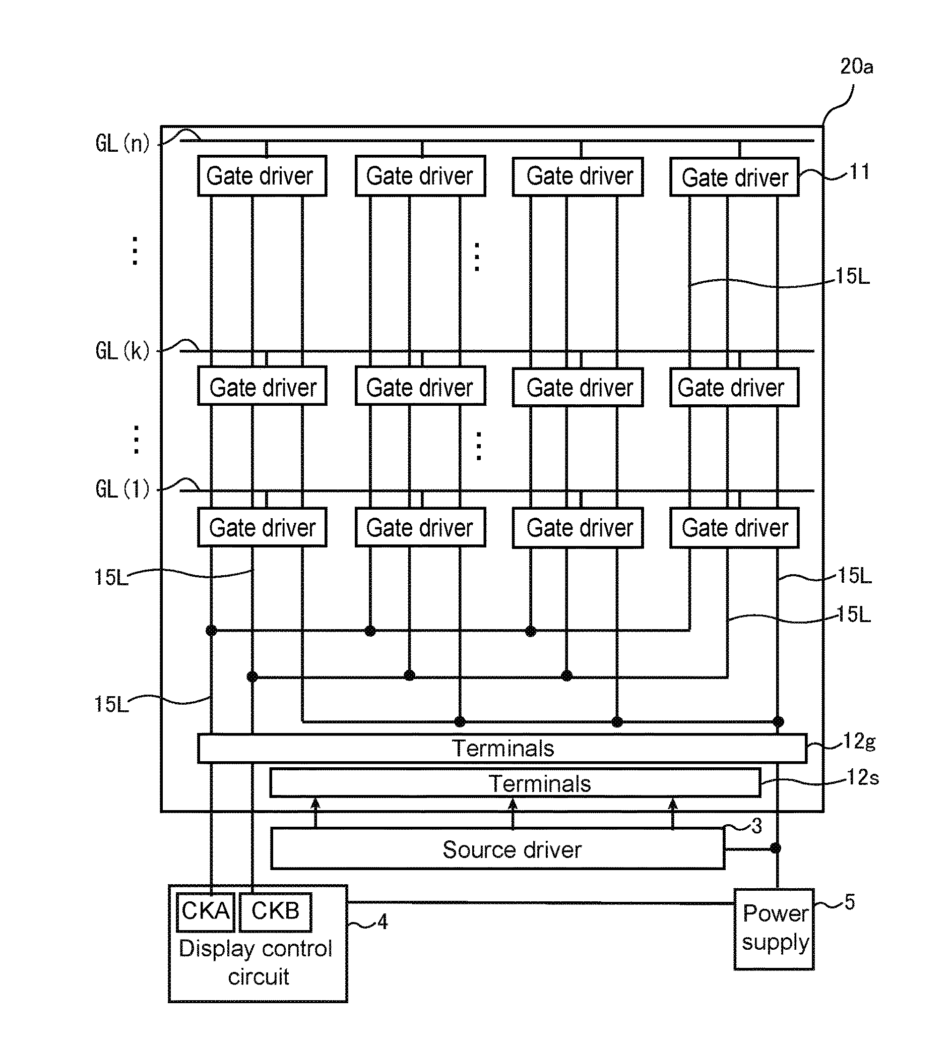
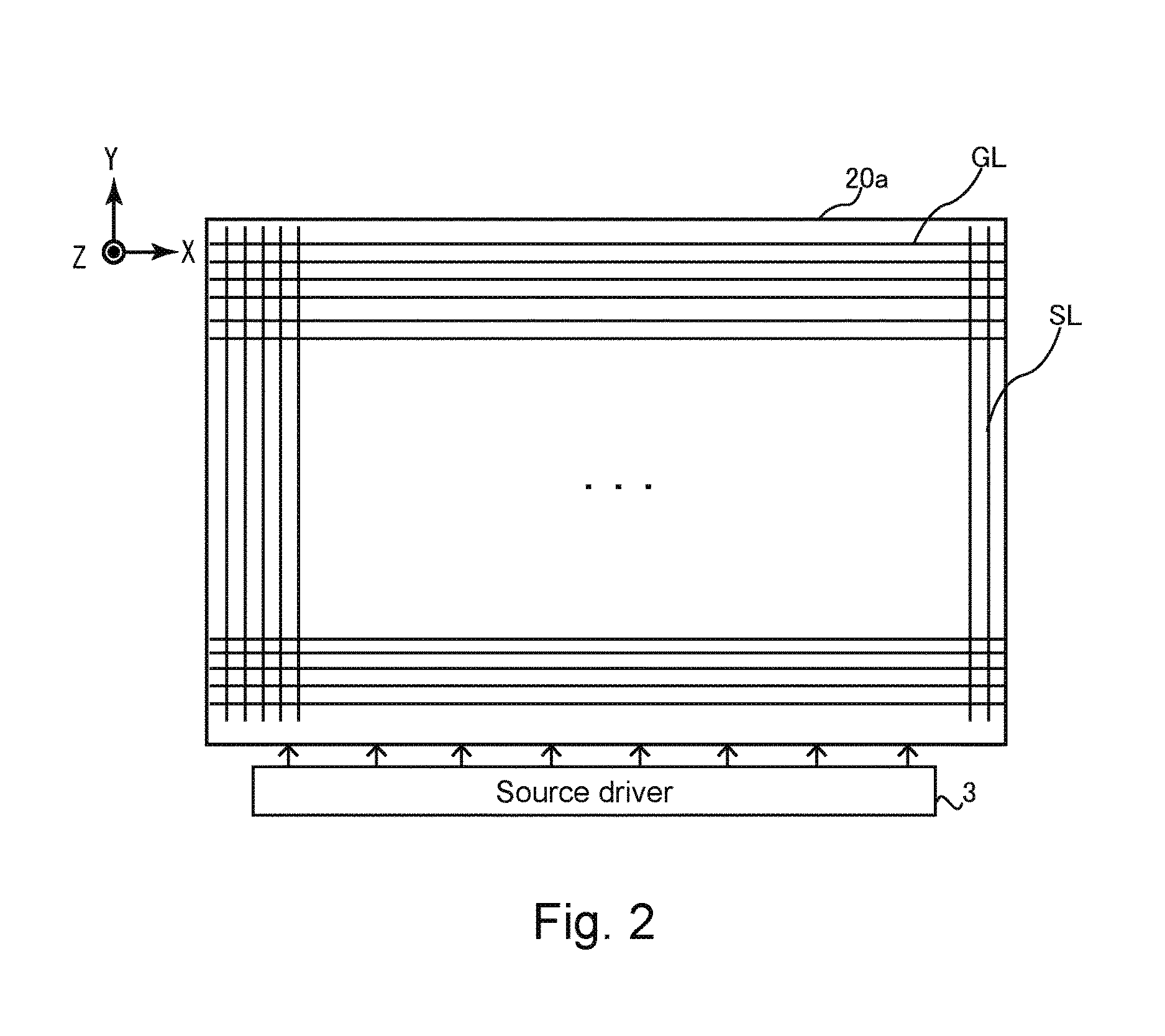
[0087]The liquid crystal display device 1 includes a display panel 2, a source driver 3, a display control circuit 4, and a power supply 5. The display panel 2 includes an active-matrix substrate 20a, a counter substrate 20b, and a liquid crystal layer (not depicted) enclosed between these substrates.

[0088]The active-matrix substrate 20a is electrically connected to the source driver 3. The source driver 3 is provided on a flexible substrate or the like. The display control circuit 4 is electrically connected to the display panel 2, the source driver 3, and the power supply 5. The display control circuit 4 transmits a control signal to the source driver 3 and gate drivers 11 (see FI...

Example

Second Embodiment

[0156]The first embodiment refers to the case where the lines 17A and 17B extending from the lines 15L for transmission of the clock signals CKA and CKB cross the source lines SL. The second embodiment will refer to a measure against noise in a case where the netAs cross the source lines SL.

[0157]The gate drivers 11 will be described in terms of their disposition in the display region with reference to FIG. 20. FIG. 20 is a schematic diagram depicting disposition of the gate drivers 11 in the display region. FIG. 20 includes alphabets A to J corresponding to the TFT-A to the TFT-J depicted in FIG. 4.

[0158]The elements of the gate drivers 11 disperse between adjacent two of the gate lines GL. FIG. 20 exemplifies a case where the elements of the gate driver 11(k−1), the elements of the gate driver 11(k), the elements of the gate driver 11(k+1), and the elements of the gate driver 11(k+2) are disposed in the pixels PIX in a same column. The TFT-A to the TFT-J of the ga...

Example

Third Embodiment

[0164]The first embodiment refers to the case where the lines 17A and 17B extending from the lines 15L for transmission of the clock signals CKA and CKB cross the source lines SL. The third embodiment will refer to a measure against noise in a case where the netBs cross the source lines SL.

[0165]The gate drivers 11 will be described in terms of their disposition in the display region with reference to FIG. 23. FIG. 23 is a schematic diagram depicting disposition of the gate drivers 11 in the display region. FIG. 23 includes alphabets A to J corresponding to the TFT-A to the TFT-J depicted in FIG. 4.

[0166]The elements of the gate drivers 11 disperse between adjacent two of the gate lines GL. FIG. 23 exemplifies a case where the elements of the gate driver 11(k−1), the elements of the gate driver 11(k), the elements of the gate driver 11(k+1), and the elements of the gate driver 11(k+2) are disposed in the pixels PIX in a same column. The TFT-A to the TFT-J of the gate...


PUM


Abstract

Provided is a display device causing less noise on a signal. A display device (10) includes a plurality of signal lines (SL), a plurality of gate lines (GL), and a driving unit. The plurality of gate lines crosses the plurality of signal lines. The driving unit is connected to the plurality of gate lines and controls a potential of each of the gate lines. The driving unit includes a plurality of gate drivers (11) and a plurality of lines. The gate drivers are disposed in a display region, and at least one of the gate drivers is connected to each of the gate lines. The lines are each provided with a potential for operation of one of the gate drivers. Each of the lines crosses one of the signal lines. The plurality of lines includes a first line (17A) and a second line (17B). The driving unit switches a potential of the first line at predetermined timing. The driving unit switches a potential of the second line into a direction opposite to a direction of the switched potential of the first line upon switching the potential of the first line.

Description

TECHNICAL FIELD[0001]The present invention relates to a display device, and more particularly to a measure against noise of a signal contributory to image display.BACKGROUND ART[0002]A display device having a display region in a shape other than a rectangular shape has recently been proposed in order for design improvement. Examples of such a display device include a planar display device disclosed in JP 5299730 B1.[0003]The planar display device includes display device elements disposed linearly and continuously on a display device substrate. The display device elements include a unit circuit and a pixel circuit. The unit circuit configures a scanning circuit. The pixel circuit is connected to an output node of the unit circuit.DISCLOSURE OF INVENTION[0004]The planar display device has a large number of nodes between lines for transmission of a clock signal driving the scanning circuit and lines for transmission of a data signal indicating a pixel tone. A parasitic capacitance is p...

Claims


Application Information

Patent Timeline
IPC IPC(8): G09G3/36G02F1/1343G02F1/1368G02F1/1362
CPCG09G3/3677G09G3/3688G02F1/136286G02F1/134309G02F1/1368G09G2300/0809G02F2001/136295G09G2320/0209G09G2330/021G09G2300/0426G02F2201/121G02F2201/123G09G2310/08G09G3/20G09G3/36G09G2310/0281G02F1/136295
Inventor NISHIYAMA, TAKAYUKITANAKA, KOHHEINOMA, TAKESHIYONEBAYASHI, RYO
Owner SHARP KK
Why Eureka
Try Eureka