Lighting Device and Method for Producing a Lighting Device

a technology of lighting device and light source, which is applied in the direction of semiconductor devices, diodes, electrical apparatus, etc., can solve the problems of optical disturbance for observers, and achieve the effect of simplifying and shortening the production process

Inactive Publication Date: 2017-02-23
OSRAM OLED
View PDF9 Cites 6 Cited by
  • Summary
  • Abstract
  • Description
  • Claims
  • Application Information

AI Technical Summary

Benefits of technology

[0021]This brings about the technical effect, in particular, that a homogeneous layer thickness may be achieved. In particular, this advantageously brings about, in a simple manner, the formation of the color scattering layer in the emission area. That simplifies and shortens a production process.
[0022]In particular, masks may be used for spraying, such that only specific areas of the carrier are sprayed with the corresponding particles (conversion particles and / or color scattering particles). Spraying thus results in a particularly high flexibility with regard to design and / or geometry since in general it is necessary only to adapt the masks for different designs or geometries.

Problems solved by technology

In the case of a carrier on which for example light emitting diodes are arranged, in general color differences or inhomogeneities may occur, for example due to the substrate or the carrier, a metallization, conversion layers (for example phosphor layers), or wires, and may be perceived as optically disturbing for an observer.

Method used


Image

  • Lighting Device and Method for Producing a Lighting Device
  • Lighting Device and Method for Producing a Lighting Device
  • Lighting Device and Method for Producing a Lighting Device

Examples


Embodiment Construction

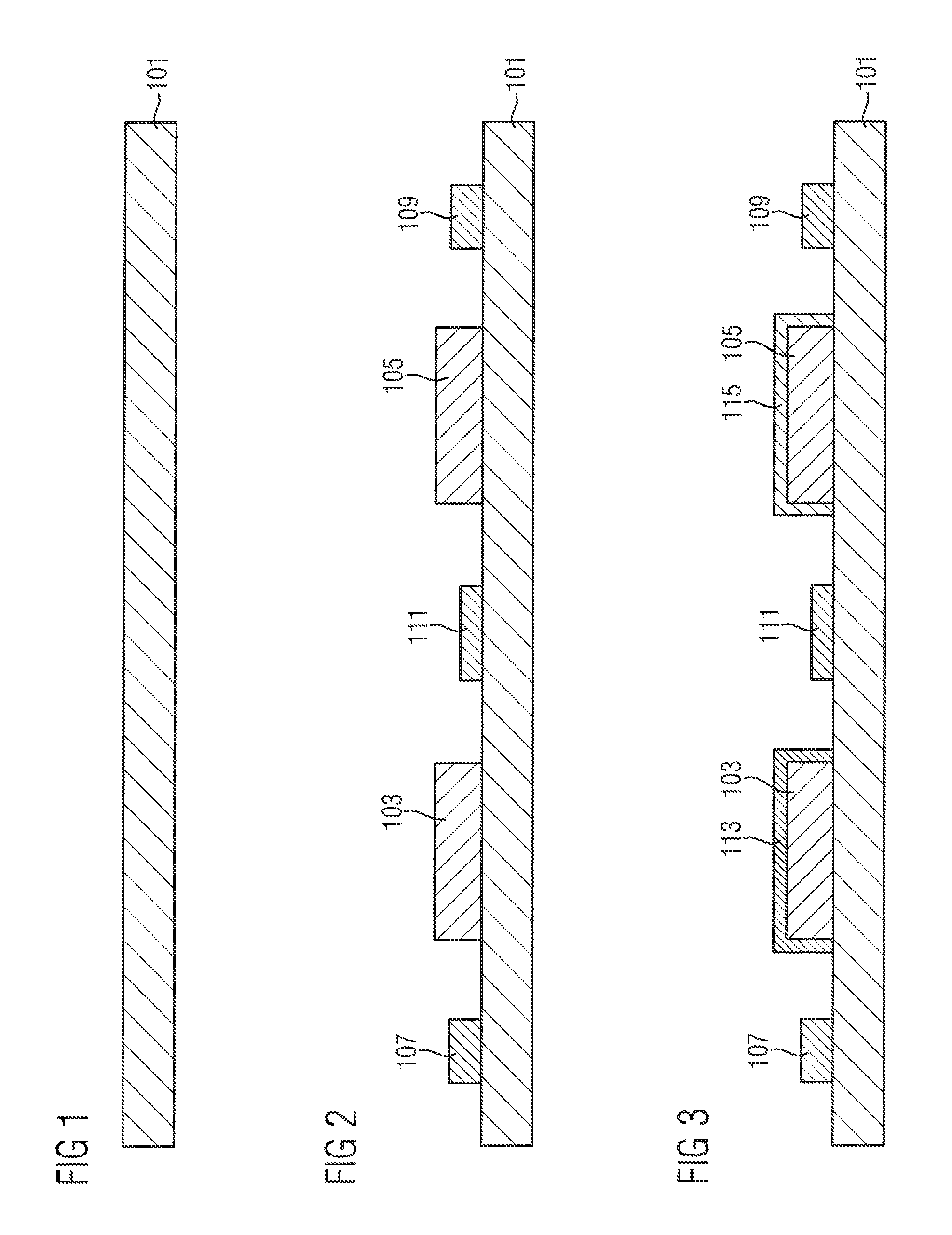
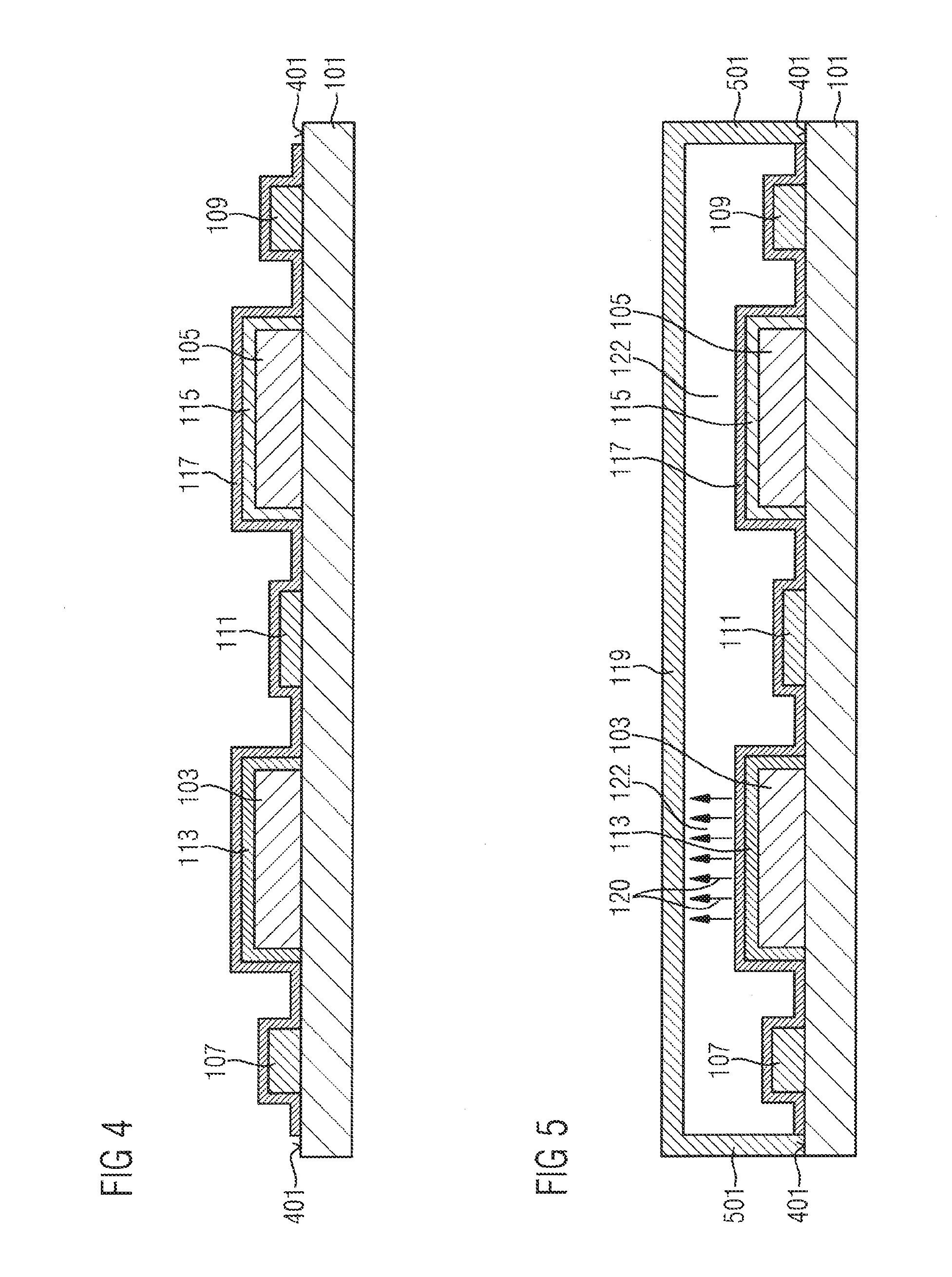
[0076]FIGS. 1 to 5 respectively show a point in time in a method for producing a lighting device.

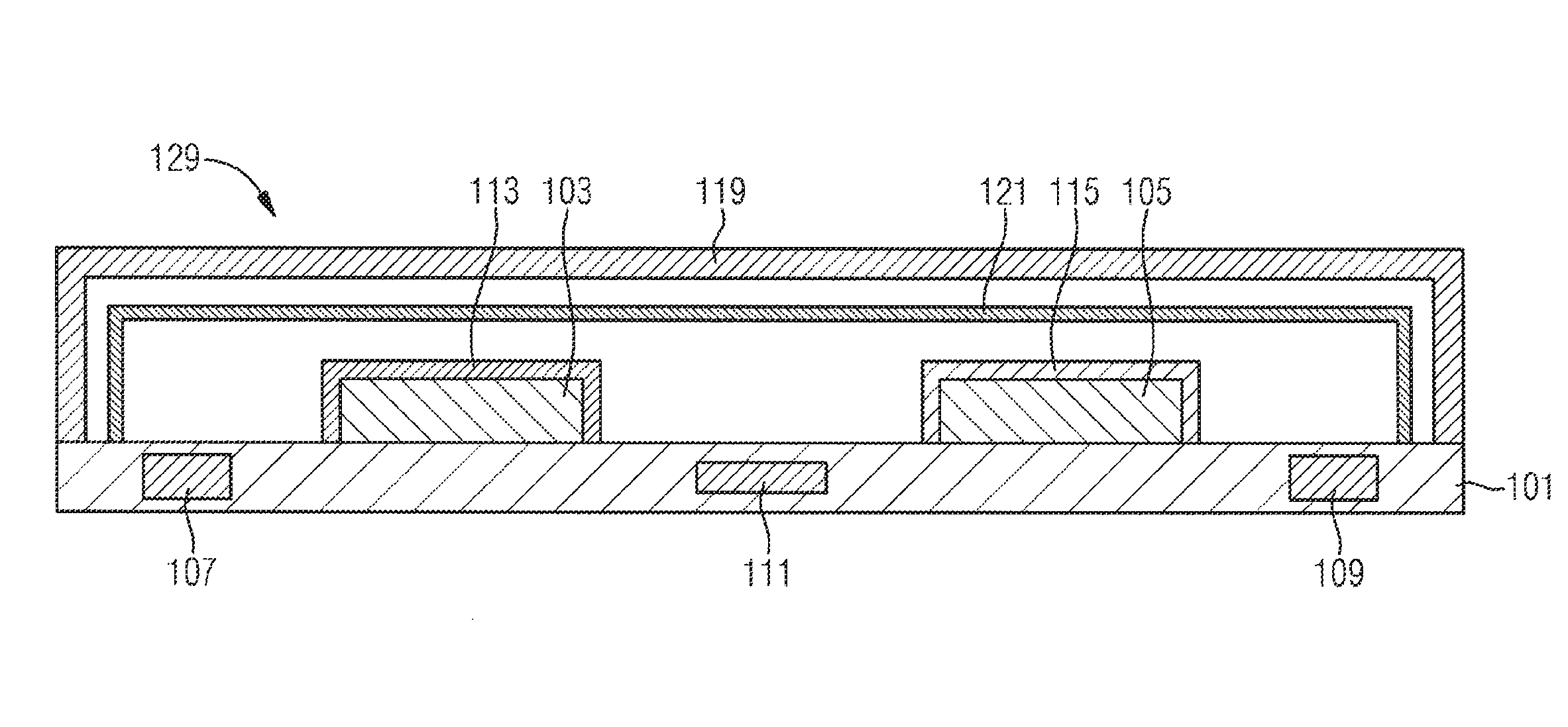
[0077]In accordance with FIG. 1, a carrier 101 is provided. The carrier 101 may be a substrate, for example. The carrier 101 may be a circuit board, for example.

[0078]In accordance with FIG. 2, two optoelectronic illuminants 103 and 105 are arranged on the carrier 101. In this case, it is provided, in particular, that the two optoelectronic illuminants 103, 105 are electrically wired with the carrier 101. This is the case particularly if the carrier 101 is a circuit board. Analogously, two protective diodes 107 and 109 and a temperature sensor 111 as electronic components are arranged on the carrier 101 and electrically wired with the latter. The electrical wiring is generally designated as “wire bonding”. In an exemplary embodiment which is not shown, more or fewer than two illuminants 103, 105 may be provided. In a further exemplary embodiment which is not shown, further electronic com...


PUM


Abstract

A lighting device and a method for producing a lighting device are disclosed. In an embodiment, the lighting device includes a carrier, at least one optoelectronic illuminant arranged on the carrier, the illuminant configured to emit light into an emission area and a color scattering layer located in the emission area, the color scattering layer configured to generate a color by scattering of light at a surface of the color scattering layer facing away from the illuminant.

Description

[0001]This patent application is a national phase filing under section 371 of PCT / EP2015 / 059455, filed Apr. 30, 2015, which claims the priority of German patent application 10 2014 106 074.1, filed Apr. 30, 2014, each of which is incorporated herein by reference in its entirety.TECHNICAL FIELD[0002]The invention relates to a lighting device and to a method for producing a lighting device.BACKGROUND[0003]In the case of a carrier on which for example light emitting diodes are arranged, in general color differences or inhomogeneities may occur, for example due to the substrate or the carrier, a metallization, conversion layers (for example phosphor layers), or wires, and may be perceived as optically disturbing for an observer. This is the case particularly when the light emitting diode is switched off, that is to say is not emitting light.[0004]Therefore, there is a need to reduce or even completely avoid inhomogeneities in the optical impression.SUMMARY OF THE INVENTION[0005]Embodime...

Claims


Application Information

Patent Timeline
Patent Type & Authority Applications(United States)
IPC IPC(8): H01L51/52H01L51/56H01L27/02H01L27/32
CPCH01L51/5268H01L51/5237H01L27/0248H01L51/5275H01L51/56H01L27/322H01L25/0753H01L33/44H01L33/505H01L2924/00H01L2924/0002H10K50/854H10K50/84H10K50/858H10K59/38H10K71/00
Inventor RACZ, DAVIDSPATH, GUENTERRICHTER, MARKUS
Owner OSRAM OLED
Why Eureka
Try Eureka