Wafer leveling device

a leveling device and wafer technology, applied in the direction of basic electric elements, semiconductor/solid-state device manufacturing, electric devices, etc., can solve the problem of bringing more stresses to the wafer, and achieve the effect of reducing stresses on the surface of the wafer

Active Publication Date: 2017-03-02
E&R ENG CORP
View PDF3 Cites 5 Cited by
  • Summary
  • Abstract
  • Description
  • Claims
  • Application Information

AI Technical Summary

Benefits of technology

[0012]In view of the above issues, the present disclosure describes a wafer leveling device which relies on a claw component, a base component and a ring component to level and stabilize a wafer and a dynamic module to ascend / descend a wafer effectively.
[0013]The present disclosure is to provide a wafer leveling device with multiple components for reducing stresses on the surface of a wafer.
[0014]The present disclosure is to provide a wafer leveling device which prevents a wafer from any contact damage between the wafer and the wafer leveling device by means of auxiliary feed-in units made of bevel soft material.
[0015]The present disclosure is to provide a wafer leveling device which removes possible shifts of a wafer to be leveled by means of magnetic components.
[0016]The present disclosure is to provide a wafer leveling device which relies on three groups of motors to drive a wafer for up / down movements without instability of the wafer.
[0027]In contrast to conventional techniques, a wafer leveling device in the present disclosure has advantages as follows: (1) less stress on the surface of a wafer; (2) less damage to a wafer which is contacted by a wafer leveling device; (3) applications of magnetic components for fewer shifts of a wafer during leveling.

Problems solved by technology

However, pressures are applied on front and back rims of a warped wafer during calibrations by two planes at which there is no flexible space but bring more stresses on the wafer.

Method used


Image

  • Wafer leveling device
  • Wafer leveling device
  • Wafer leveling device

Examples


Embodiment Construction

[0040]A wafer leveling device will be further illustrated in preferred embodiments for clear understanding of purposes, characteristics and effects:

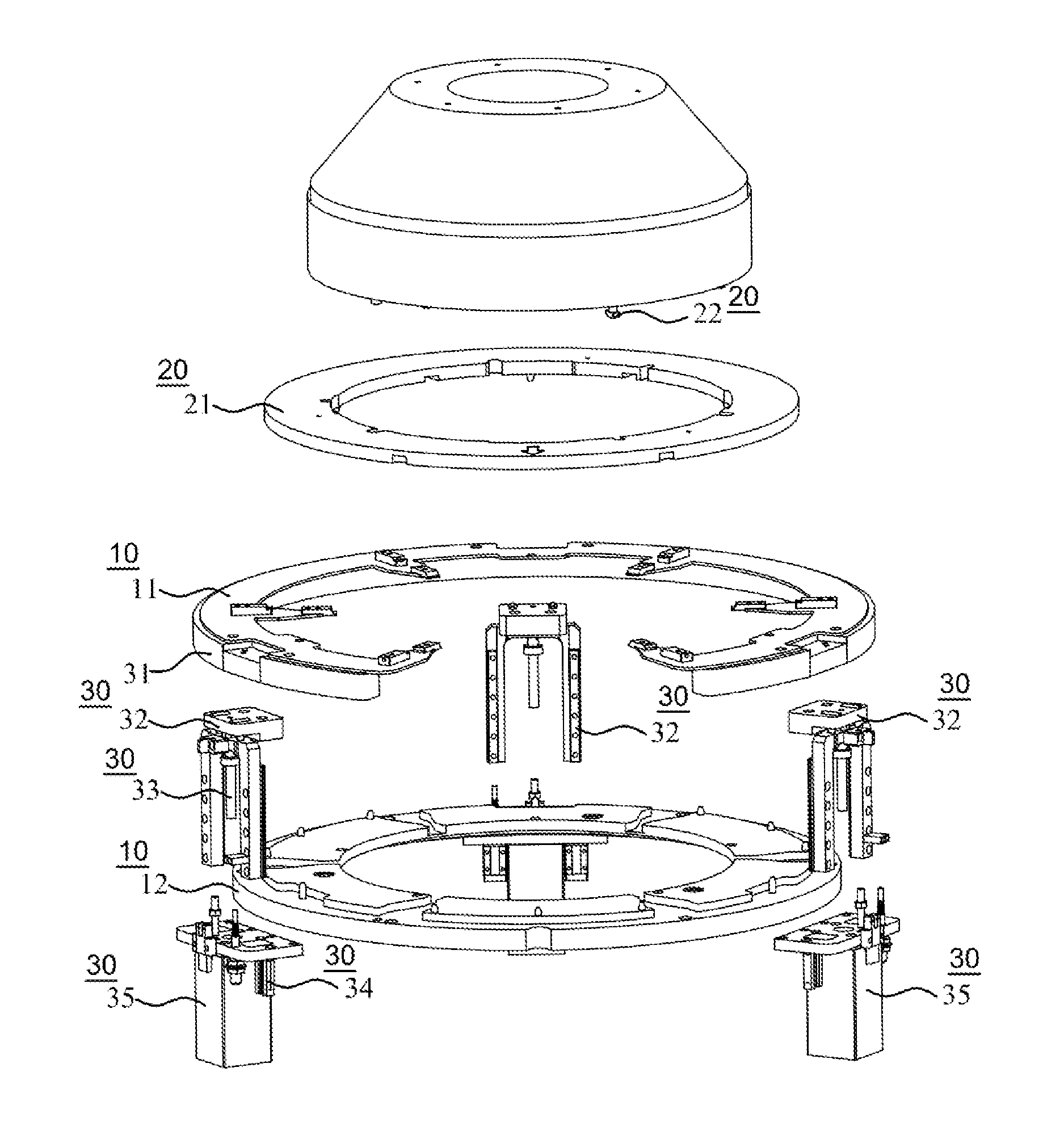
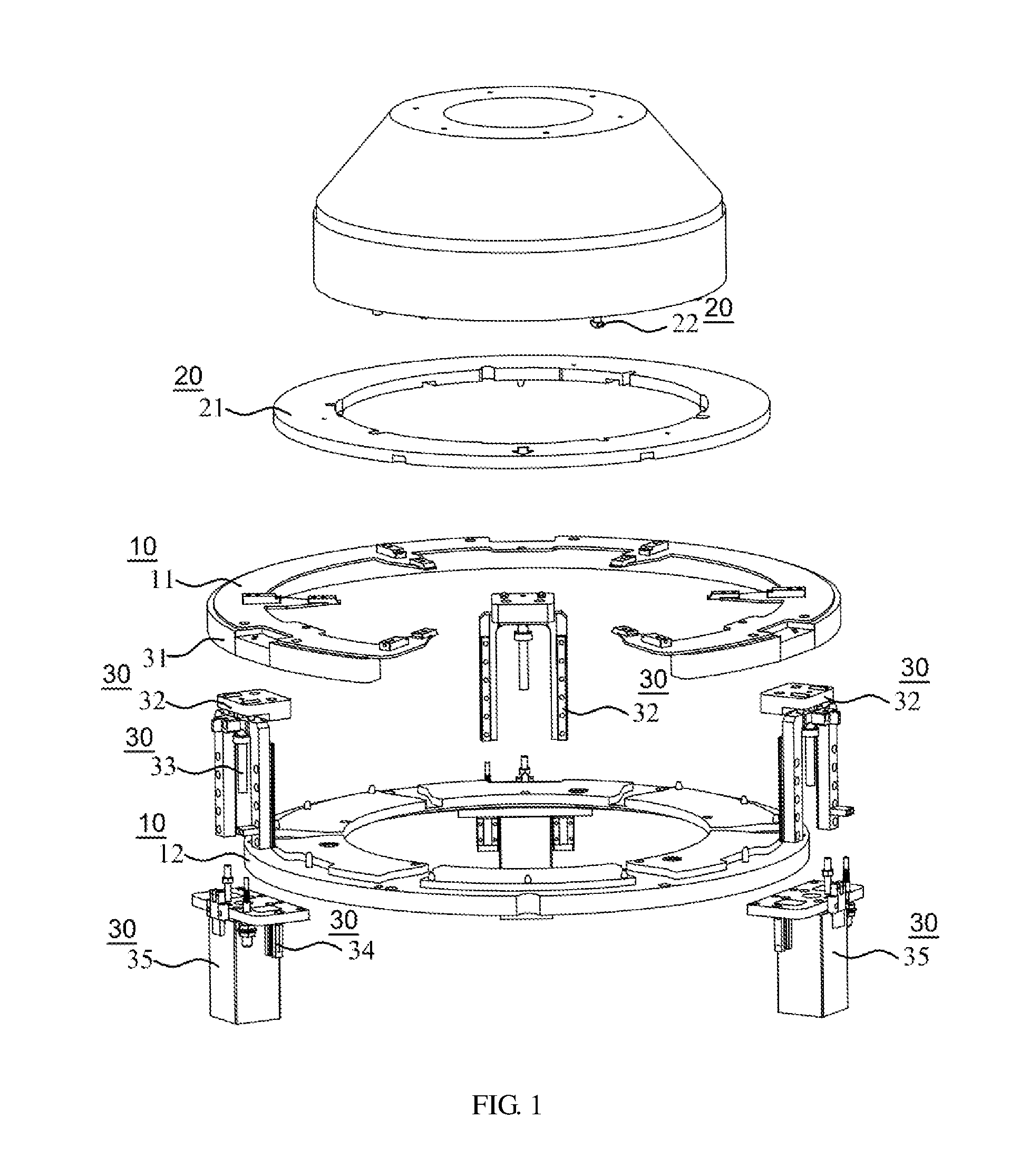
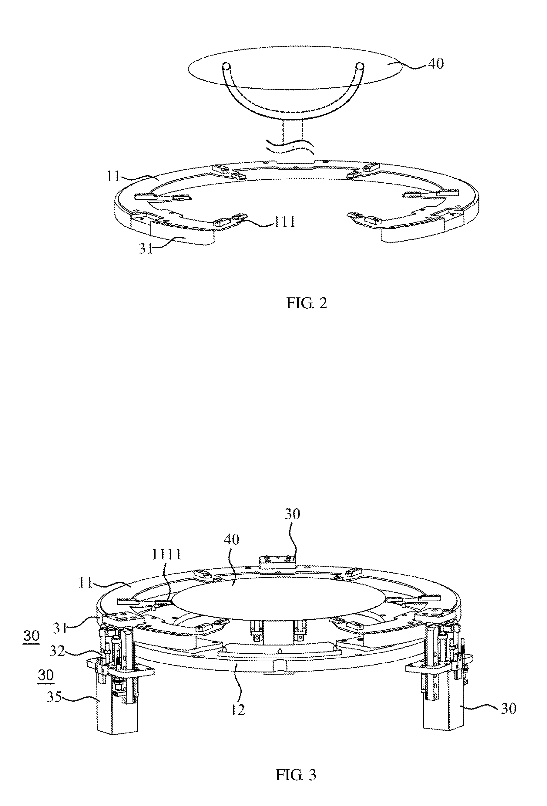
[0041]FIG. 1 to FIG. 11 present a wafer leveling device in preferred embodiments. Referring to FIG. 1 which illustrates a wafer leveling device comprises a carrier module (10), a fixture module (20) and a dynamic module (30): the carrier module (10) comprises a claw component (11) and a base component (12); the fixture module (20) comprises a ring component (21) and a clamp component (22).

[0042]Specifically, as shown in FIG. 1, the carrier module (10), which is a load-bearing module under a wafer, is divided into the claw component (11) and the base component (12). As shown in FIG. 2, the edges of several claw structures (111) at the claw component (11) lifted by the dynamic modules (30) (not shown in the figure) contact the bottom surface of the wafer (40), which has been conveyed to and stays above the claw component (11) by a robotic ...


PUM


Abstract

The present disclosure relates to a wafer leveling device which comprises a carrier module, a fixture module and a dynamic module. A wafer, which is conveyed to and stays above a claw component of the carrier module by a robotic arm, is further carried by the lifted claw component for a continuous ascent until the wafer is contacted by a ring component of the fixture module; the clamp component of the fixture module releases the ring component; the claw component, the ring component and the wafer, all of which keep stabilized mutual positions, are lowered so that several protrudent structures on a base component of the carrier module contact the wafer; the claw component, the ring component and the wafer which completes a manufacturing process are lifted; the carrier module and the wafer are lowered with the clamp components stabilizing the ring component.

Description

BACKGROUND OF THE INVENTION[0001]1) Field of the Invention[0002]The present disclosure relates to a wafer leveling device which enhances flatness of a wafer during a manufacturing process and particularly flatness of a large-sized or thinned wafer which is warped and goes against precision of a manufacturing process for the wafer.[0003]2) Description of the Prior Art[0004]In recent years, smart phones have been a part of every consumer's life in addition to all types of wearable devices getting more popular with the general public. It can be seen from the trend of consumer goods that merchandise is being miniaturized for strengthened computing power.[0005]Basically, the consumer goods are electronic devices characteristic of compact sizes and good computing power, both of which can be promoted with manufacturing processes based on the well-known “Moore's Law”. In semiconductor manufacturing processes, the laser marking process depends on the laser beam to label marks on wafers for t...

Claims


Application Information

Patent Timeline
Patent Type & Authority Applications(United States)
IPC IPC(8): H01L21/67H01L21/683H01L21/687
CPCH01L21/67092H01L21/6838H01L21/67259H01L21/68735H01L21/67288H01L21/68785
Inventor WU, WEN RENCHUNG, CHO CHUN
Owner E&R ENG CORP
Why Eureka
Try Eureka