

Display device
a display device and display technology, applied in the field of display devices, can solve the problems of decreasing luminance or varied chromaticity to be visible, and achieve the effects of poor viewing angle characteristics, decreased luminance, and varied chromaticity
- Summary
- Abstract
- Description
- Claims
- Application Information
AI Technical Summary
Benefits of technology
Problems solved by technology
Method used
Image

Examples
embodiment 1
[0060]In this embodiment, structure examples of a display device of one embodiment of the present invention will be described.
[0061]The display device of one embodiment of the present invention includes a plurality of pixels. Each pixel includes a display element and a coloring layer for coloring light from the display element. An electrode (e.g., a pixel electrode) of the display element and the coloring layer can be provided to face each other. The coloring layers in adjacent pixels are arranged apart from each other.
[0062]In addition, a structure body is positioned between two coloring layers in adjacent pixels. The structure body can be positioned, for example, between two pixels corresponding to different colors.
[0063]The display device can have a structure, for example, in which a display element, a coloring layer, and a structure body are interposed between a pair of substrates. For example, one of the substrates can be provided with an electrode of the display element and th...
structure example 1
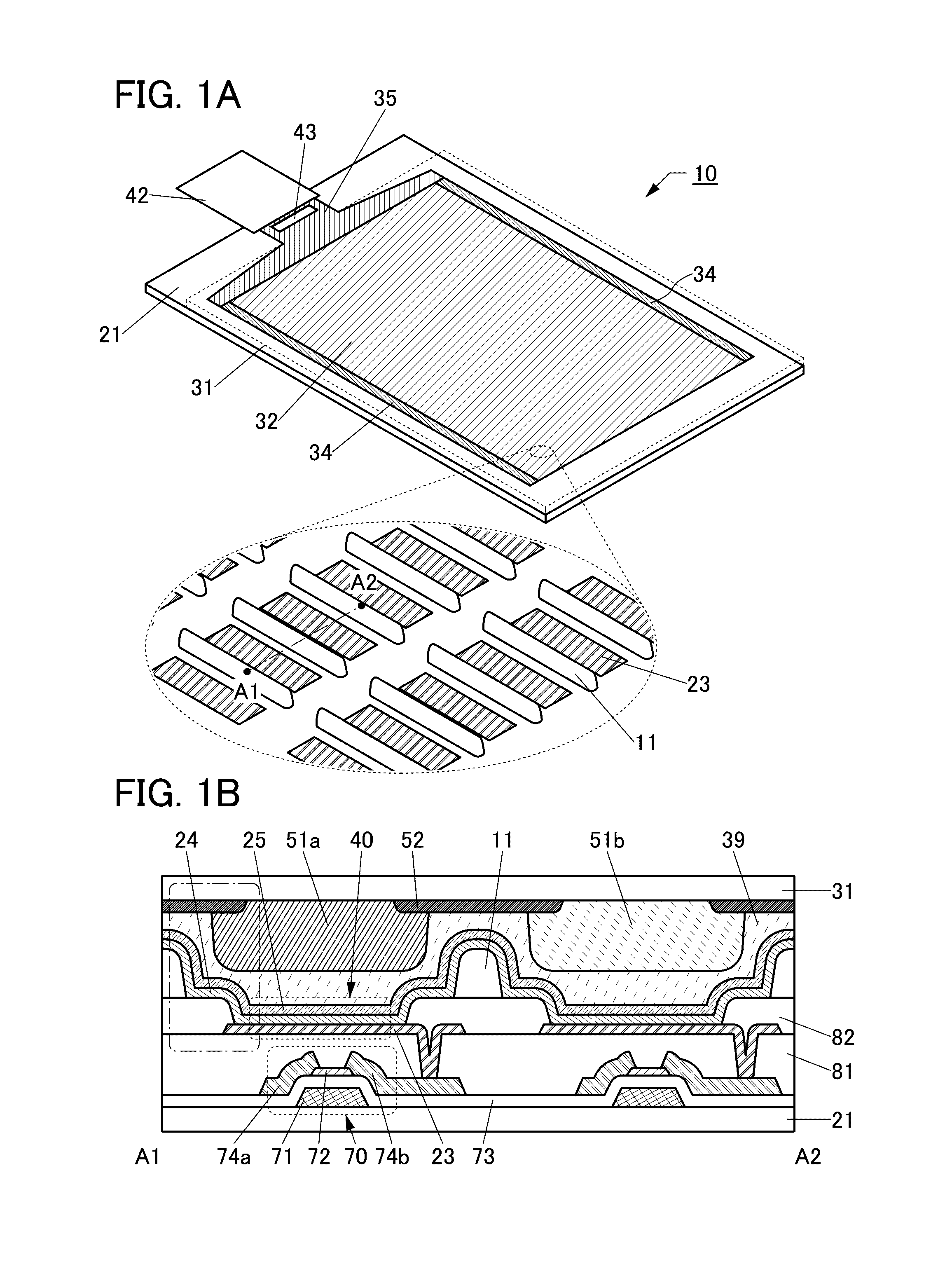
[0070]FIG. 1A is a schematic perspective view illustrating a display device 10 of one embodiment of the present invention. The display device 10 includes a substrate 21 and a substrate 31 which are bonded to each other. In FIG. 1A, the substrate 31 is denoted by a dashed line.
[0071]The display device 10 includes a display portion 32, circuits 34, a wiring 35, and the like. For example, a conductive layer 23, which is included in the circuit 34, the wiring 35, and the display portion 32 and serves as a pixel electrode, is provided on the substrate 21. FIG. 1A shows an example in which an IC 43 and an FPC 42 are mounted on the substrate 21.
[0072]A circuit serving as a scan line driver circuit can be used as the circuit 34, for example.
[0073]The wiring 35 is configured to supply a signal or electric power to the display portion 32 or the circuit 34. The signal or electric power is input to the wiring 35 from the outside through the FPC 42 or from the IC 43.
[0074]In FIG. 1A, the IC 43 i...
example 1
CROSS-SECTIONAL STRUCTURE EXAMPLE 1
CROSS-SECTIONAL STRUCTURE EXAMPLE 1-1
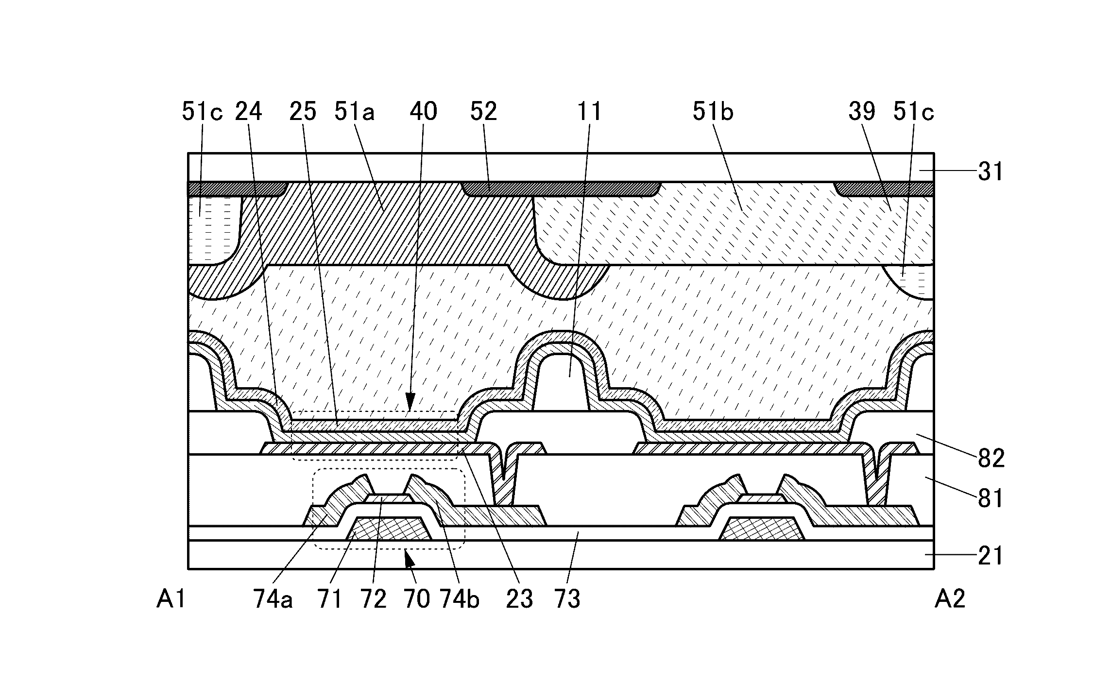
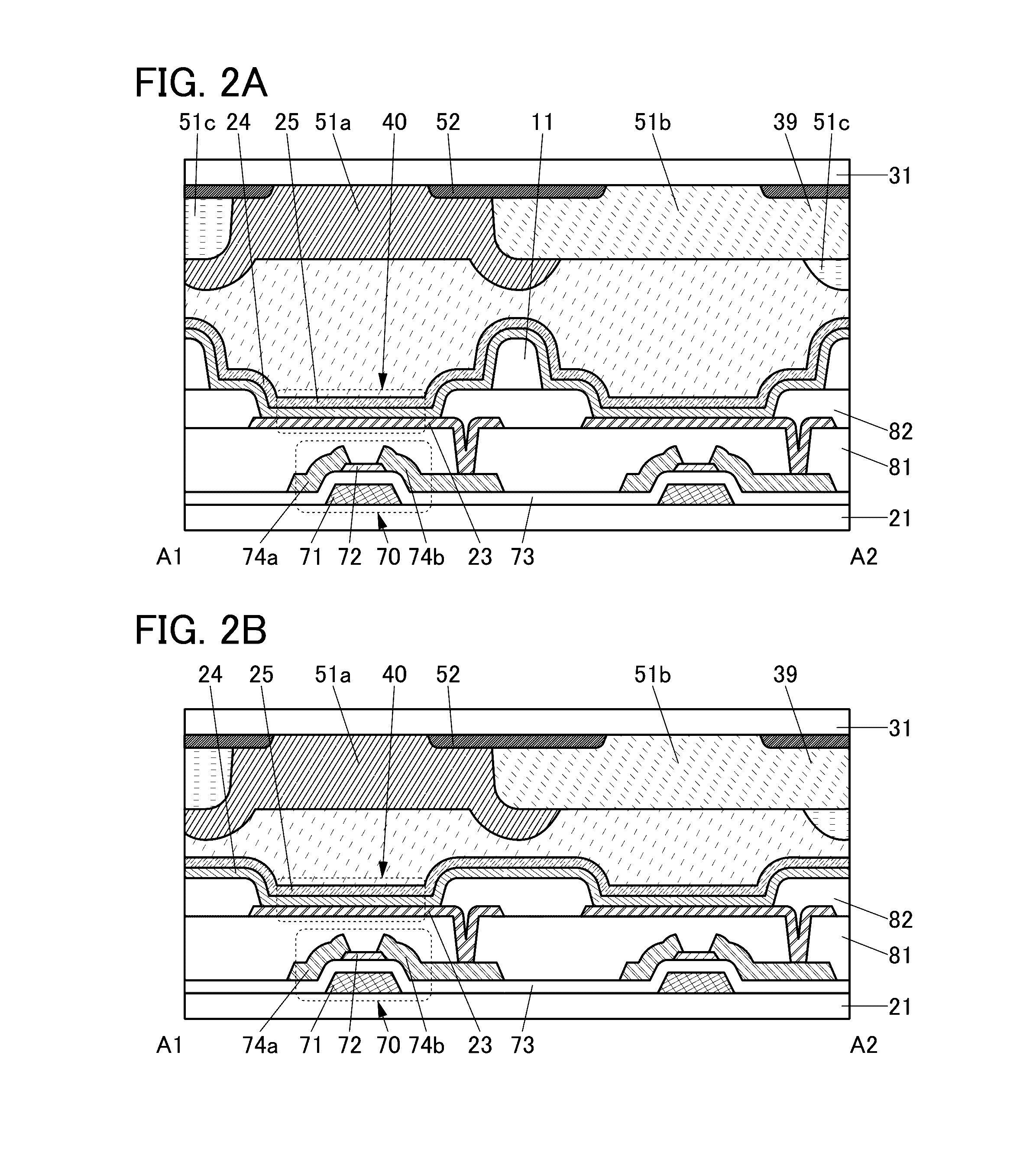
[0076]FIG. 1B shows an example of a cross section along line A1-A2 in FIG. 1A. FIG. 1B shows the cross section of a region including two adjacent pixels (sub-pixels). In this example, a light-emitting element 40 with a top-emission structure is used as a display element; thus, the display surface is on the side of the substrate 31.
[0077]The display device 10 has a structure in which the substrate 21 and the substrate 31 are bonded with an adhesive layer 39. In other words, the light-emitting element 40 is sealed with the adhesive layer 39.
[0078]A transistor 70, the light-emitting element 40, the structure body 11, and the like are provided over the substrate 21. In addition, insulating layers 73, 81, 82, and the like are provided over the substrate 21. On the surface of the substrate 31 that faces the substrate 21, provided are a coloring layer 51a, a coloring layer 51b, a light-blocking layer 52, and the like.
[...
PUM
 Abstract
Description
Claims
Application Information