
Plasma Excitation for Spatial Atomic Layer Deposition (ALD) Reactors

Active Publication Date: 2017-03-09
LAM RES CORP
View PDF65 Cites 14 Cited by
  • Summary
  • Abstract
  • Description
  • Claims
  • Application Information

AI Technical Summary

Benefits of technology

[0022]In accordance with the embodiments disclosed, by moving the RF power with the shuttle, deposition can be efficiently conducted in a spatial ALD arrangement without the drawbacks of leading edge thickness variations, trailing edge contamination and/or feature surface co

Problems solved by technology

Throughput of the typical ALD system is limited.
The limitations of gas switching technology, as well as the time required to purge the single substrate showerhead and reactor introduce inherent delays.
As this plasma front moves over the substrate, it can induce currents that can lead to device damage.
Spatial ALD systems also suffer in that deposited materials over the leading edge of the substrate, due to longer residence time under the plasma, may become thicker (e.g., tilt in the deposition layer) than the trailing edge of the substrate.
Another problem is that the trailing edge can be exposed to the precurs

Method used


Image

  • Plasma Excitation for Spatial Atomic Layer Deposition (ALD) Reactors
  • Plasma Excitation for Spatial Atomic Layer Deposition (ALD) Reactors
  • Plasma Excitation for Spatial Atomic Layer Deposition (ALD) Reactors

Examples


Example

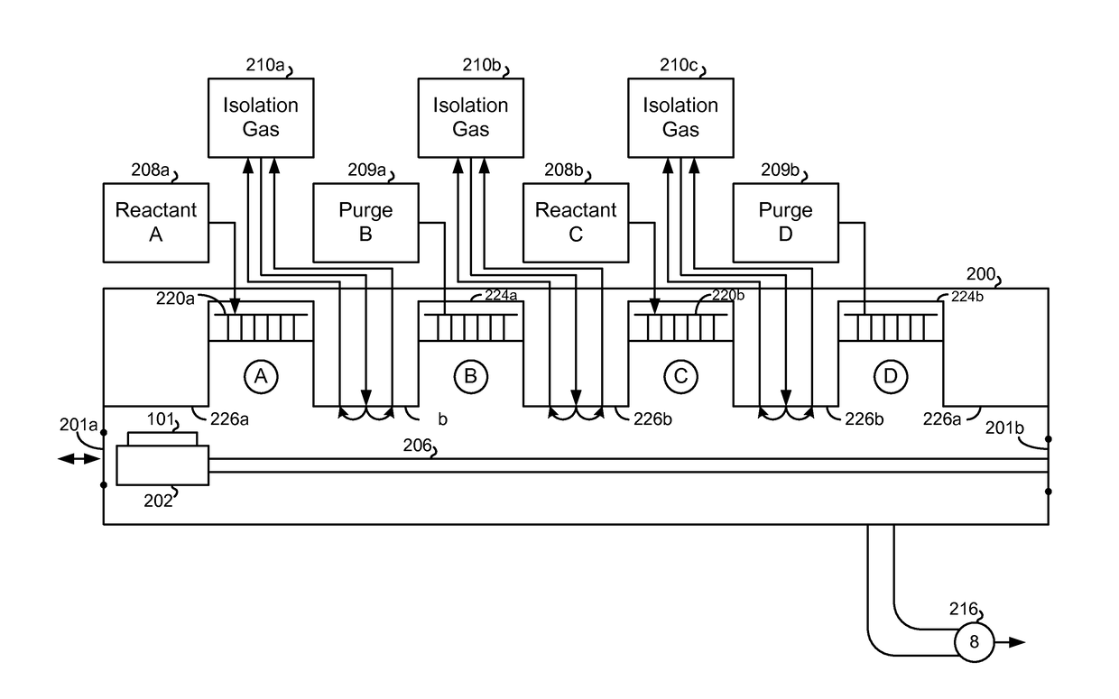
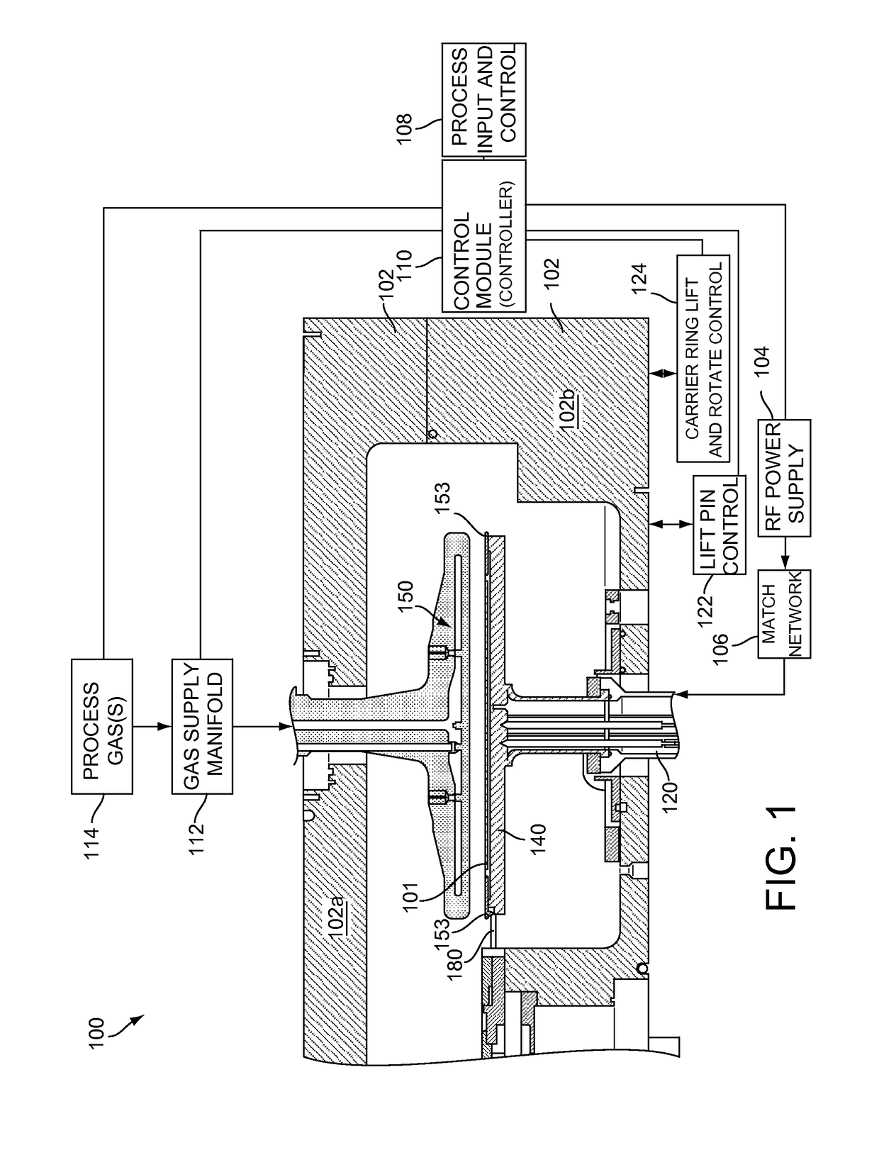
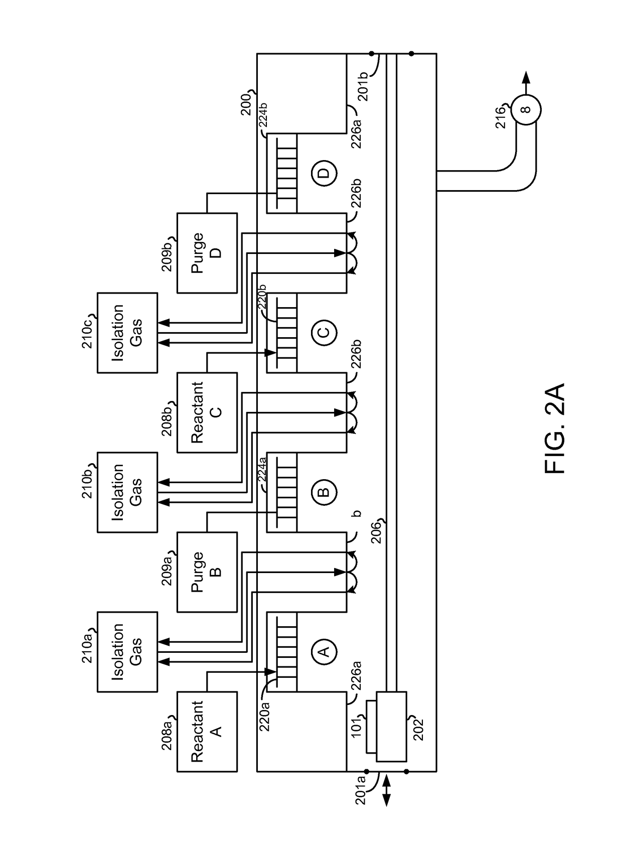
[0032]Embodiments of the disclosure provide examples of atomic layer deposition (ALD) reactors that operate as spatial ALD reactors, wherein rather than bringing reactants to the substrate, the substrate is moved to the reactants instead. For example, in one spatial ALD configuration, the reactants are brought to the substrate (or vice versa) in space. The reactants and substrate need to move relative to each other. In one embodiment, the radio frequency (RF) excitation comes from the substrate side and moves with the substrate, eliminating moving plasma fronts that can cause current imbalances and device damage. In one embodiment, moving the substrate with the RF excitation can occur by translating the substrate linearly or rotating the substrate about an axis distal to the substrate center. In the examples provided herein, without limitation to other ways of moving the substrate and RF excitation, a shuttle that supports the substrate is linearly or circularly moved along a track....


PUM

PropertyMeasurementUnit
Heightaaaaaaaaaa
Poweraaaaaaaaaa
Heightaaaaaaaaaa

Abstract

A spatial atomic layer deposition (ALD) system is disclosed. The system includes a chamber that includes a plurality of zones oriented along a track. Also included is a shuttle that is configured to support the substrate and transport the substrate to each of the plurality of zones to enable deposition of a thin film. The shuttle includes an RF power electrode and an RF ground electrode coupled to an RF power source. The RF electrode and the RF ground electrode are each embedded in the shuttle, such that power provided by the RF power source to the shuttle moves with the shuttle to each of the zones. The RF power source is configured to be activated in synchronization with moving the shuttle to one of the zones.

Description

BACKGROUND[0001]1. Field of the Disclosure[0002]The present embodiments relate to semiconductor substrate processing methods and equipment tools, and more particularly, atomic layer deposition (ALD) systems that enable spatial ALD with a moving RF source.[0003]2. Description of the Related Art[0004]Atomic layer deposition (ALD), also known as atomic layer chemical vapor deposition (ALCVD), is a method for producing very thin films that are highly conformal, smooth, and possess excellent physical properties. ALD uses volatile gases, solids, or vapors that are sequentially introduced (or pulsed) over a heated substrate. A first precursor is introduced as a gas, which is absorbed (or adsorbed) into the substrate and the reactor chamber is cleared of the gaseous precursor. A second precursor is introduced as a gas, which reacts with the absorbed precursor to form a monolayer of the desired material. By regulating this sequence, the films produced by ALD are deposited a monolayer at a ti...

Claims


Application Information

Patent Timeline
IPC IPC(8): C23C16/455C23C16/509C23C16/52H01J37/32C23C16/458
CPCC23C16/4554H01J2237/3323C23C16/45519H01J37/32091H01J37/32568H01J37/32743H01J37/32788C23C16/458H01J37/32715H01J37/3244C23C16/52C23C16/509H01J2237/3321H01J2237/327C23C16/45551C23C16/45542C23C16/4586H01L21/0228H01L21/02315H01L21/28194H01L21/3065H05H1/46C23C14/56C23C14/564C23C14/568C23C16/4401C23C16/45521C23C16/4583C23C16/56H01L21/67155H01L21/67161H01L21/67173
Inventor LEESER, KARL F.
Owner LAM RES CORP
Learn More