Source-driving circuit and liquid crystal display (LCD) panel thereof

Inactive Publication Date: 2017-03-09
TCL CHINA STAR OPTOELECTRONICS TECH CO LTD +1
View PDF6 Cites 1 Cited by
  • Summary
  • Abstract
  • Description
  • Claims
  • Application Information

AI Technical Summary

Benefits of technology

[0054]The present invention provides a source-driving circuit and LCD panel thereof. The gamma voltage output module of the source-driving circuit in the present invention is used to output a plurality of reference voltage signals having an equal duration interval to the digital-to-analog converter; each reference voltage signal comprises a gamma reference voltage signal; at least one reference voltage signal further comprises a low voltage signal wherein a voltage value of the low voltage signal is less than that of the gamma reference voltage signal; a duration interval of the reference voltage signal is equal to that of a current gamma reference voltage signal

Problems solved by technology

Conventionally, with the increased resolution of the small to medium panel sizes in the mobile phones, an inadequate power-charging phenomenon of the pixel unit on the display panel occurs if the original charging technology is used to charge the high resolution panel.
However, a common issue existing in these solutions is that the power consumption of the high resolution pane

Method used


Image

  • Source-driving circuit and liquid crystal display (LCD) panel thereof
  • Source-driving circuit and liquid crystal display (LCD) panel thereof
  • Source-driving circuit and liquid crystal display (LCD) panel thereof

Examples


Example

Embodiment 1

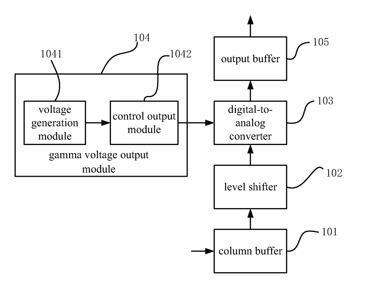
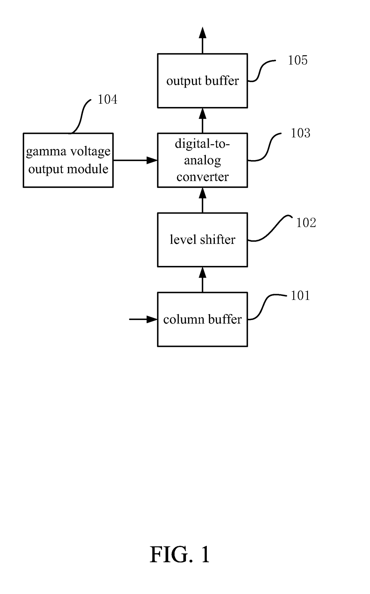
[0059]In order to reduce the power consumption of the high resolution panel, the present invention provides a source-driving circuit, as shown in FIG. 1. The source-driving circuit comprises a column buffer 101, a level shifter 102, a digital-to-analog converter 103, a gamma voltage output module 104 and an output buffer 105.

[0060]The column buffer 101 is used to store the inputted video signal and outputs the stored video signal to the level shifter.

[0061]The level shifter 102 is used to amplify the voltage of the video signal for activating the digital-to-analog converter 103.

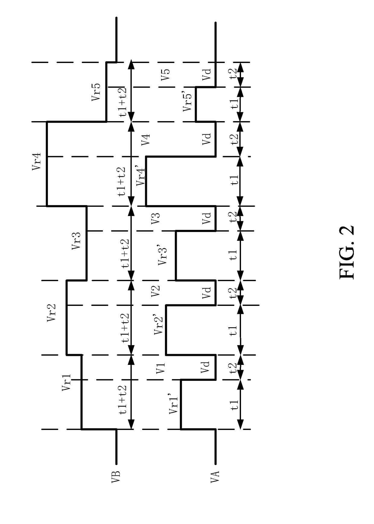
[0062]The gamma voltage output module 104 is used to output the reference voltage signals having the equal duration intervals to the digital-to-analog converter 103 wherein each reference voltage signal comprises a gamma reference voltage signal. At least one reference voltage signal further comprises a low voltage signal wherein the voltage value of the low voltage signal is less than that of the...

Example

Embodiment 2

[0082]The present invention provides a LCD panel comprising: an array substrate including a plurality of scanning lines, a plurality of data lines and plurality of pixel units; the scanning lines used to transmit scanning signals; the data lines used to transmit gray level voltage signals; the pixel units defined by interlacing the scanning lines and the data lines for displaying the screen based on the scanning signals and the gray level voltage signals; and a source-driving circuit comprising a column buffer, a level shifter, a digital-to-analog converter, an output buffer and a gamma voltage output module.

[0083]The column buffer is used to store the inputted video signal and outputs the stored video signal to level shifter.

[0084]The level shifter is used to amplify the voltage of the video signal for activating the digital-to-analog converter.

[0085]The gamma voltage output module 104 is used to output the reference voltage signals having the equal duration intervals t...


PUM


Abstract

The present invention provides a source-driving circuit and LCD panel thereof. In the source-driving circuit, the reference voltage signal outputted by the gamma voltage output module comprises a gamma reference voltage signal and a low voltage signal, wherein the voltage value of the low voltage signal is less than that of the gamma reference voltage signal, and the duration interval of the reference voltage signal is equal to that of the current gamma reference voltage signal. In comparison to the conventional technique, the power consumption of the source-driving circuit is reduced and the power consumption of the high resolution display panel is further decreased.

Description

BACKGROUND OF THE INVENTION[0001]Field of Invention[0002]The present invention relates to a technical field of a liquid crystal display (LCD), and more particularly to a source-driving circuit and LCD panel thereof.[0003]Description of Prior Art[0004]Conventionally, with the increased resolution of the small to medium panel sizes in the mobile phones, an inadequate power-charging phenomenon of the pixel unit on the display panel occurs if the original charging technology is used to charge the high resolution panel.[0005]In the light of inadequate power-charging phenomenon of the pixel unit on the display panel, many conventional techniques provide some mature solutions. However, a common issue existing in these solutions is that the power consumption of the high resolution panel is severely increased. For the electronic apparatuses such as mobile phones, the standby time of the battery has been widely criticized. The wattage consumption rises and thus, the standby time of the electr...

Claims


Application Information

Patent Timeline
IPC IPC(8): G09G3/20G02F1/1362G09G3/36
CPCG09G3/2011G09G3/3696G09G3/3685G09G3/3674G02F1/136286G09G2330/021G09G2310/0224G09G2310/0251G09G2310/0289G09G2310/0291G09G2320/0276G09G2310/027
Inventor XING, ZHENZHOUXOAPING, TANXINGLING, GUO
Owner TCL CHINA STAR OPTOELECTRONICS TECH CO LTD
Why Eureka
Try Eureka