System for conversion between analog domain and digital domain with mismatch error shaping

a technology of mismatch error and conversion system, applied in the field of system for conversion between analog domain and digital domain with mismatch error shaping, can solve the problems of mismatch error and the inapplicability of the dac system b>100/b> for fast conversion

Active Publication Date: 2017-03-16
MEDIATEK INC
View PDF13 Cites 11 Cited by
  • Summary
  • Abstract
  • Description
  • Claims
  • Application Information

AI Technical Summary

Benefits of technology

[0010]In an embodiment (e.g., FIGS. 9 to 10 or FIGS. 12 to 13b), the system receives a first input analog value (e.g., Vi′ in FIG. 10 or 13a / 13b) and outputs a first output digital value (e.g., D′ or D′op in FIG. 10 or 13a / 13b) converted from the first input analog value during a first cycle (e.g., 1000′ or 1300′), and receives a second input analog value (e.g., Vi) and outputs a second output digital value (e.g., D or Dop in FIG. 9 or 12) converted from the second input analog value during a second cycle (e.g., 1000 or 1300), wherein the subset of bits (e.g., {d′[N−1], . . . , d′[0]} of the first digital value (e.g., D′ in FIG. 10 or 13a / 13b) is extracted from the first output digital value; the system further comprises a register (e.g., 940 or 1240), the first injection circuit comprises an additional control circuit (e.g., 950 or 1250) coupled to the register, and the DAC comprises a peripheral circuit (e.g., 930 or 1230) coupled to the register, and a plurality of capacitors (e.g., c[N] to c[0]). Each of the capacitors has a top terminal coupled to a common node (e.g., nz1 or nz2), and a bottom terminal coupled to the peripheral circuit. During a first phase (e.g., 1002a or 1302a) of the second cycle, the additional control circuit controls the register to register the subset of bits of the first digital value, and controls the peripheral circuit to conduct the bottom terminals of the capacitors to voltages (e.g., −d′[n]*Vr) reflecting the subset of bits of the first digital value, and to conduct the common node to the second input analog value, so as to enable the analog injection value to be injected. During a second phase (e.g., 1002b or 1302b) of the second cycle after the first phase, the peripheral circuit conducts the bottom terminals of the capacitors to a reset voltage (e.g., V0), and the register resets. The system further includes a comparator (e.g., 910 or 1210) coupled to the common node and the register, wherein during a period (e.g., p[n] in FIG. 10 or 13b) of the second cycle, the comparator compares a voltage (e.g., Vz1 or Vz2) at the common node to set a bit (e.g., b[n]) of the register.

Problems solved by technology

However, the plurality of conversion elements suffer deviations (e.g., variations) from their expected values, and therefore introduce mismatch error during conversion.
Consequently, the DAC system 100 is not applicable for fast conversion, such as CT-DSM (continuous time delta sigma modulator).

Method used


Image

  • System for conversion between analog domain and digital domain with mismatch error shaping
  • System for conversion between analog domain and digital domain with mismatch error shaping
  • System for conversion between analog domain and digital domain with mismatch error shaping

Examples


Embodiment Construction

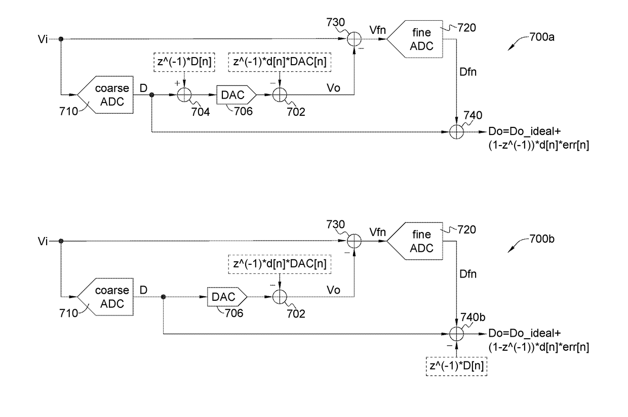
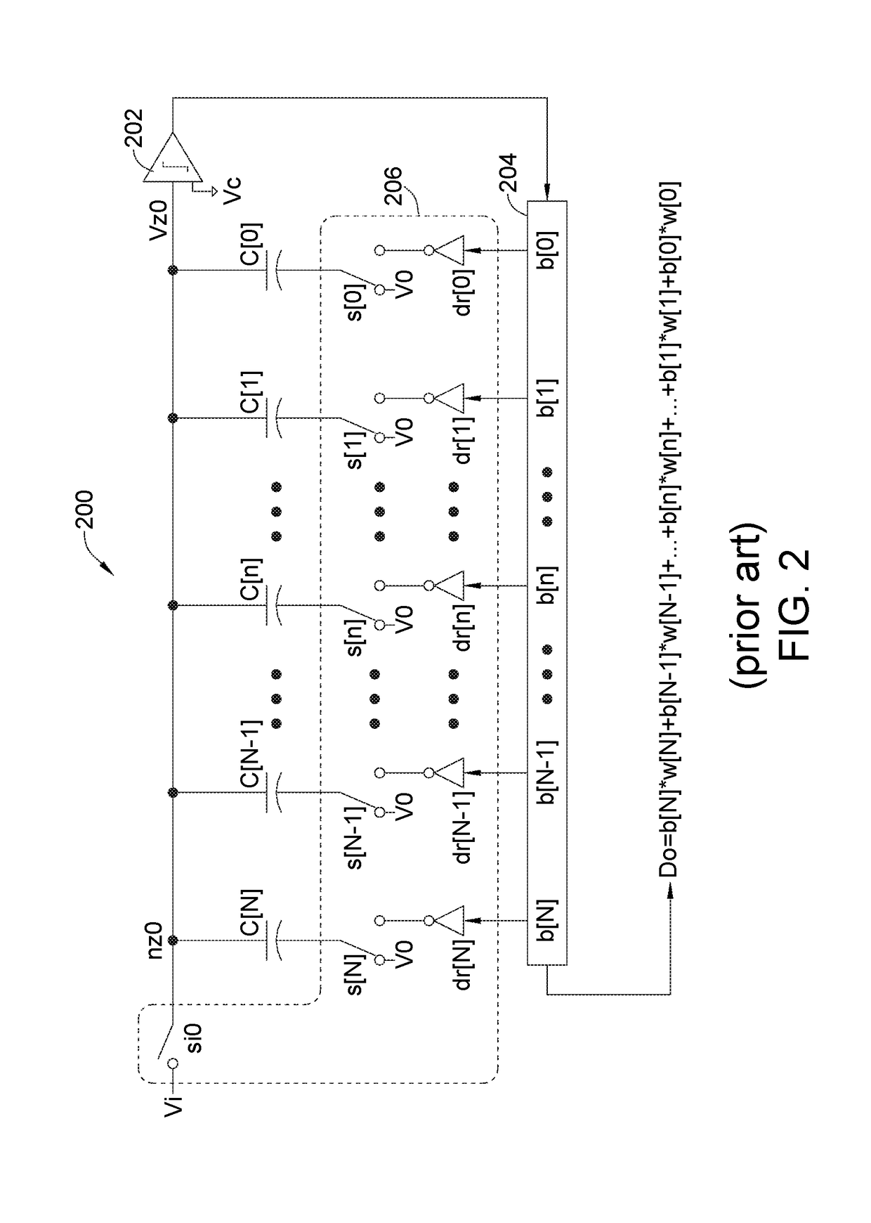
[0042]Please refer to FIGS. 2 and 3. FIG. 2 illustrates a system 200 which implements a SAR ADC for converting an analog value Vi to a digital value Do, and FIG. 3 illustrates operations of the system 200. The system 200 may include a comparator 202, a register 204, a peripheral circuit 206 and an array of capacitors C[N], C[N−1], . . . , C[1] and C[0]. The peripheral circuit 206 includes a switch si0, a plurality of switches s[N], s[N−1], . . . , s[1] and s[0], and a plurality of bias circuits dr[N], dr[N−1], . . . , dr[l] and dr[0]. The switch si0 is coupled between the analog value Vi and a node nz0. The comparator 202 is coupled to the node nz0, and capable of comparing if a voltage Vz0 at the node nz0 is greater than a voltage Vc. Each capacitor C[n] (for n=N, N−1, . . . to 0) has a top terminal coupled to the node nz0, and a bottom terminal coupled to the switch s[n] to be selectively conducted to a constant reset voltage V0 (e.g., a ground level) or the bias circuit dr[n]. Th...


PUM


Abstract

The invention provides a system for conversion between analog domain and digital domain with mismatch error shaping, including a DAC, a first injection circuit couple to the DAC, and a second injection circuit coupled to the DAC. The DAC generates a first analog value in response to a first digital value, and generates a second analog value in response to a second digital value. The first injection circuit enables an analog injection value to be injected to the second analog value when the DAC generates the second analog value, wherein the analog injection value is converted from a digital injection value formed by a subset of bits of the first digital value. The second injection circuit combines the digital injection value and one of the following: the second digital value and a related value obtained according to the second analog value.

Description

[0001]This application claims the benefit of U.S. provisional application Ser. No. 62 / 218,053, filed Sep. 14, 2015, the subject matter of which is incorporated herein by reference.FIELD OF THE INVENTION[0002]The present invention relates to a system for conversion between analog domain and digital domain with mismatch error shaping (MES), and more particularly, to a system implementing MES by injections of previous values in analog and digital domains.BACKGROUND OF THE INVENTION[0003]Semiconductor circuitry system with functionality of conversion between digital and analog domains is essential for modern electronic, e.g., mobile phone, notebook / tablet computer, digital camera / camcorder, navigation system, etc.[0004]For converting a digital input to an analog output, a DAC (digital-to-analog converter) selectively activates a subset of a plurality of conversion elements (e.g., resistors, capacitors or current sources, etc.) according to value of the digital input, so as to synthesize...

Claims


Application Information

Patent Timeline
Patent Type & Authority Applications(United States)
IPC IPC(8): H03M1/06H03M1/12
CPCH03M1/12H03M1/0617H03M1/1014H03M1/462H03M1/66H03M1/145H03M1/68H03M3/338H03M3/344H03M1/0673H03M1/001H03M1/066
Inventor SHU, YUN-SHIANG
Owner MEDIATEK INC
Why Eureka
Try Eureka