Semiconductor Device for Detecting Fluorescent Particles

Active Publication Date: 2017-03-23
INTERUNIVERSITAIR MICRO ELECTRONICS CENT (IMEC VZW)
View PDF7 Cites 19 Cited by
  • Summary
  • Abstract
  • Description
  • Claims
  • Application Information

AI Technical Summary

Benefits of technology

[0004]It is an object of the present invention to provide a compact fluorescence dete

Problems solved by technology

However, state of the art fluorescent detectors contain different co

Method used


Image

  • Semiconductor Device for Detecting Fluorescent Particles
  • Semiconductor Device for Detecting Fluorescent Particles
  • Semiconductor Device for Detecting Fluorescent Particles

Examples


Embodiment Construction

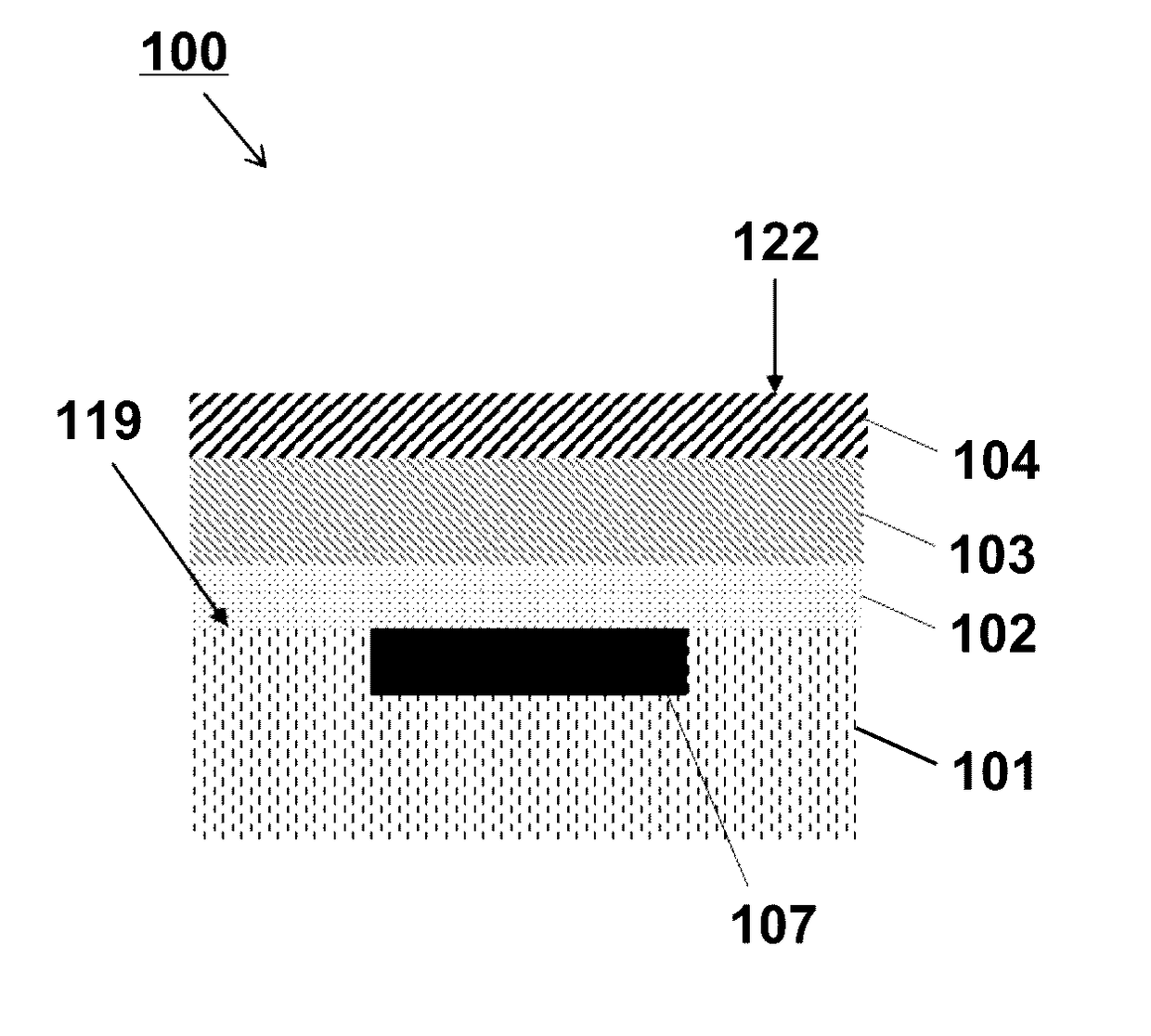
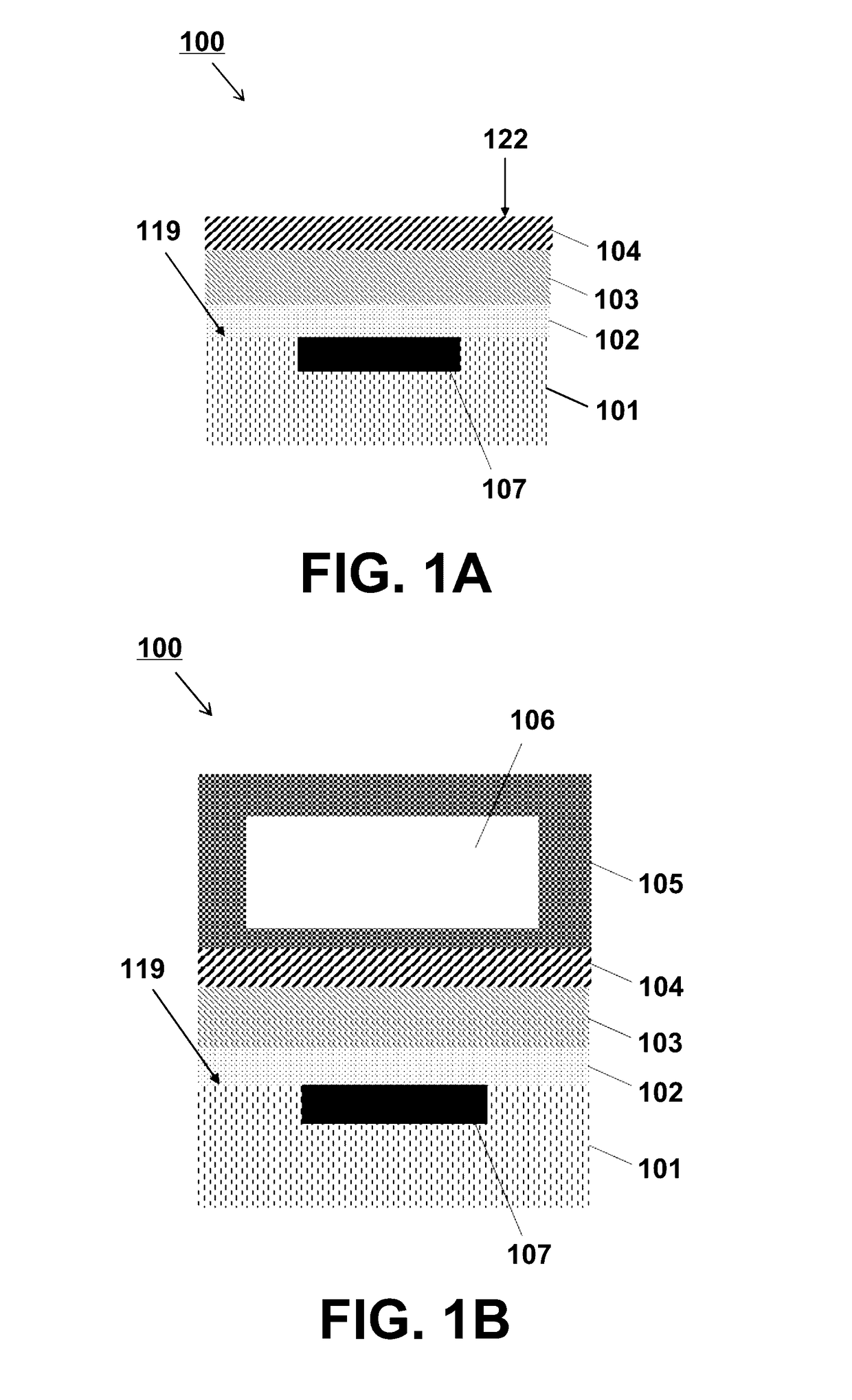
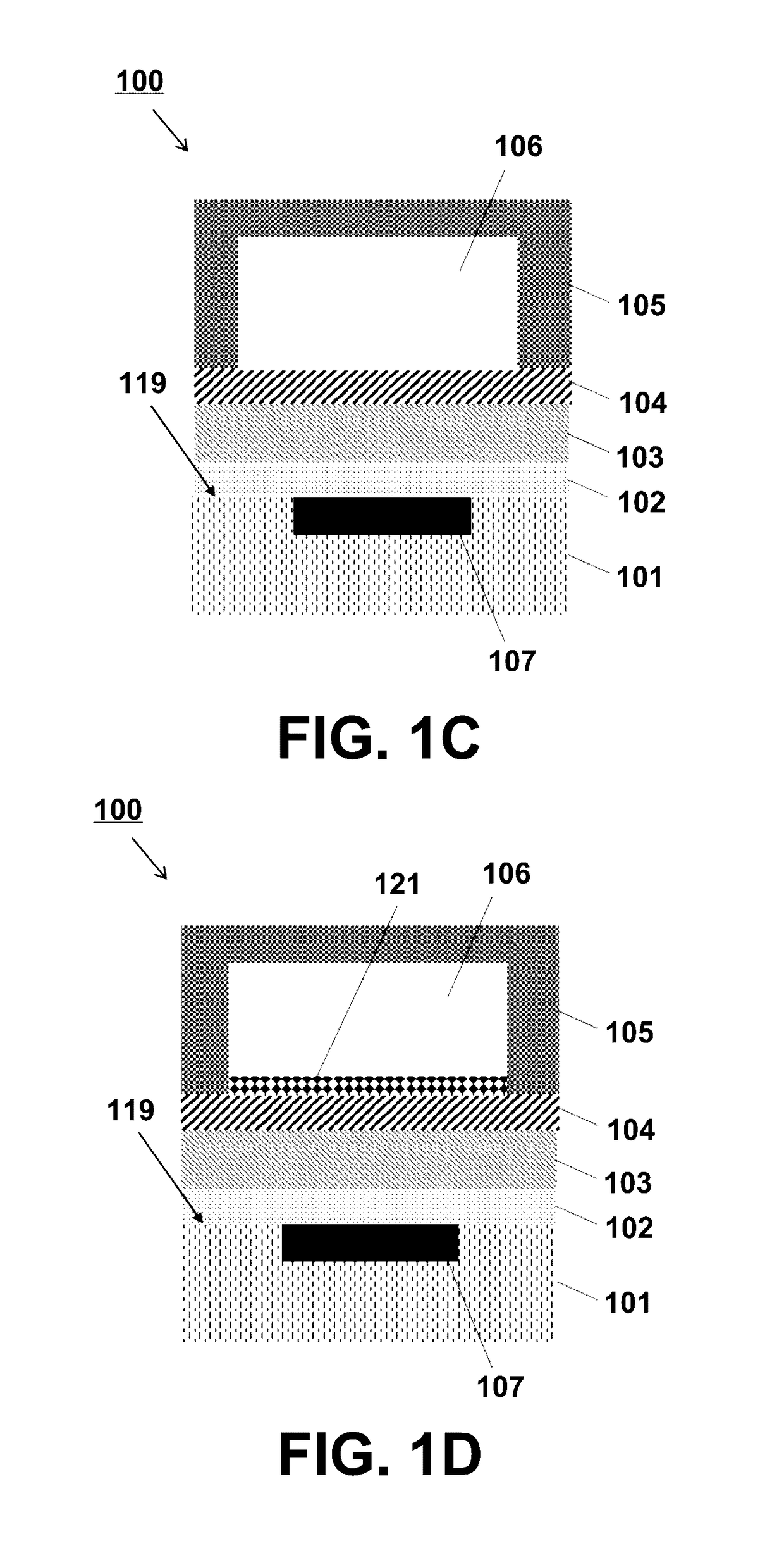
[0070]The present disclosure will be described with respect to particular embodiments and with reference to certain drawings but the disclosure is not limited thereto but only by the claims. The drawings described are only schematic and are non-limiting. In the drawings, the size of some of the elements may be exaggerated and not drawn on scale for illustrative purposes. The dimensions and the relative dimensions do not necessarily correspond to actual reductions to practice of the disclosure. Any reference signs in the claims shall not be construed as limiting the scope. In the different drawings, the same reference signs refer to the same or analogous elements.

[0071]Furthermore, the terms first, second, third and the like in the description and in the claims, are used for distinguishing between similar elements and not necessarily for describing a sequential or chronological order. The terms are interchangeable under appropriate circumstances and the embodiments of the invention d...


PUM


Abstract

The present disclosure relates to semiconductor devices for detecting fluorescent particles. At least one embodiment relates to an integrated semiconductor device for detecting fluorescent tags. The device includes a first layer, a second layer, a third layer, a fourth layer, and a fifth layer. The first layer includes a detector element. The second layer includes a rejection filter. The third layer is fabricated from dielectric material. The fourth layer is an optical waveguide configured and positioned such that a top surface of the fourth layer is illuminated with an evanescent tail of excitation light guided by the optical waveguide when the fluorescent tags are present. The fifth layer includes a microfluidic channel. The optical waveguide is configured and positioned such that the microfluidic channel is illuminated with the evanescent tail. The detector element is positioned such that light from activated fluorescent tags can be received.

Description

FIELD OF THE INVENTION[0001]The present invention relates to a device for detecting particles. In particular, the invention relates to semiconductor devices for detecting biological particles including DNA, RNA, proteins, viral particles and cells based on fluorescence.BACKGROUND OF THE INVENTION[0002]Fluorescence detectors are sensitive detectors allowing analysis or detection of particles, for instance biological molecules. A fluorescent detection is performed for instance on fluorescent tags attached to biological molecules, enabling the identification of specific biological molecules in a sample. However, state of the art fluorescent detectors contain different components which cannot be integrated in a semiconductor process flow.[0003]There is a need for a compact fluorescence based detector which can be completely manufactured using semiconductor manufacturing processes.SUMMARY[0004]It is an object of the present invention to provide a compact fluorescence detector which can b...

Claims


Application Information

Patent Timeline
IPC IPC(8): G01N21/64
CPCG01N2201/0873G01N21/6428G01N21/6454G01N21/648G01N21/7703G01N2201/064
Inventor VAN DORPE, POLLAGAE, LIESBETPEUMANS, PETERSTASSEN, ANDIMHELIN, PHILIPPEDU BOIS, BERTSEVERI, SIMONE
Owner INTERUNIVERSITAIR MICRO ELECTRONICS CENT (IMEC VZW)
Why Eureka
Try Eureka