Semiconductor device

Active Publication Date: 2017-03-23
DENSO CORP
View PDF3 Cites 8 Cited by
  • Summary
  • Abstract
  • Description
  • Claims
  • Application Information

AI Technical Summary

Benefits of technology

[0004]As described above, in the semiconductor device of Japanese Patent Application Publication No. 2015-118991, the lifetime control region is provided so that it protrudes from the diode area into the IGBT area. That is, the lifetime control region is provided partially within the IGBT area. When the lifetime control region is provided in the IGBT area, an on-voltage of the IGBT increases and a steady-state loss is more likely to occur in the IGBT. In a case where the lifetime control region in the IGBT area is provided under the intermediate depth of the drift region (on a collector region side), the on-voltage of the IGBT increases while a switching loss of the IGBT is suppressed, as a result of which becomes advantageous for the IGBT when a switching speed is fast. On the other hand, in a ca

Problems solved by technology

When the lifetime control region is provided in the IGBT area, an on-voltage of the IGBT increases and a steady-state loss is more likely to occur in the IGBT.
Due to this, if the lifetime control region is provided to protr

Method used


Image

  • Semiconductor device
  • Semiconductor device
  • Semiconductor device

Examples


Embodiment Construction

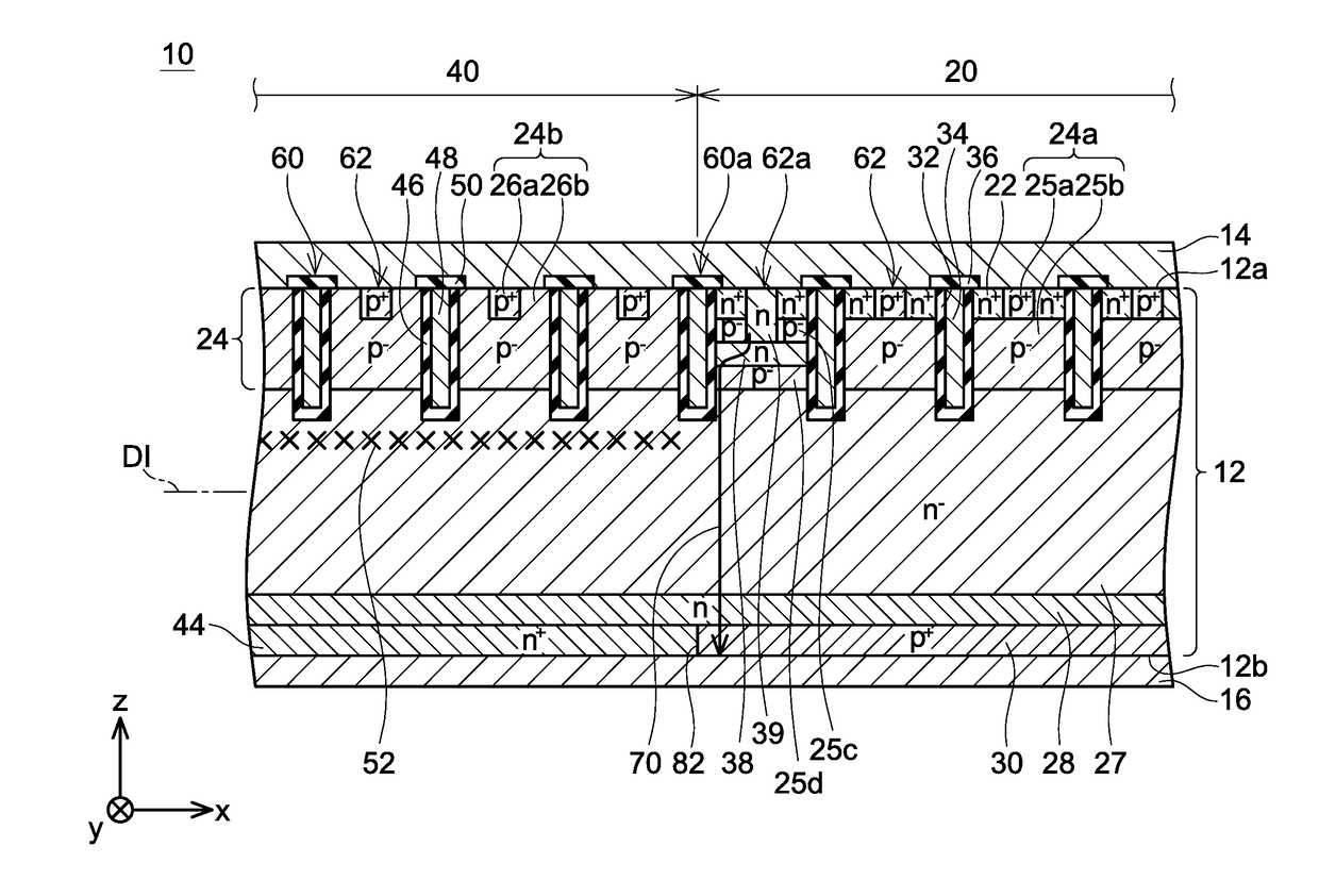
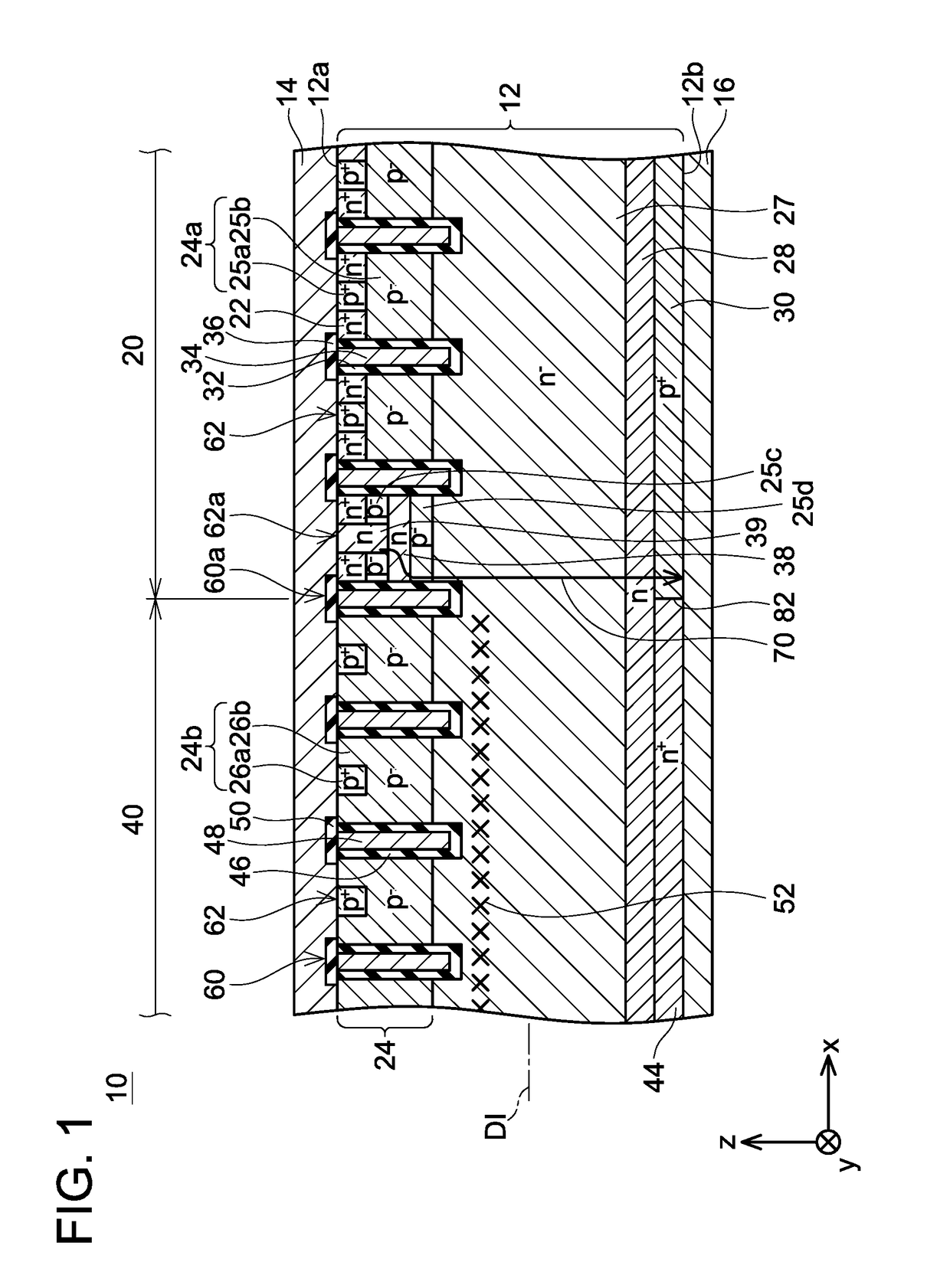
[0017]A semiconductor device 10 in an embodiment shown in FIGS. 1 to 3 comprises a semiconductor substrate 12, an upper electrode 14, and a lower electrode 16. The semiconductor substrate 12 is a substrate made of silicon. The upper electrode 14 covers an upper surface 12a of the semiconductor substrate 12. The lower electrode 16 covers a lower surface 12b of the semiconductor substrate 12. Notably, in the description below, a thickness direction of the semiconductor substrate 12 is termed a z direction, and one direction parallel to the upper surface 12a of the semiconductor substrate 12 (one direction intersecting the z direction orthogonally) is termed an x direction, and a direction that orthogonally intersects the z direction and the x direction is termed a y direction.

[0018]The semiconductor substrate 12 comprises an IGBT area 20 where a vertical type IGBT is provided, and a diode area 40 where a vertical type diode is provided. The IGBT area 20 and the diode area 40 are adjac...


PUM


Abstract

In a semiconductor device including an IGBT and a diode, an upper-side lifetime control region, which is provided in the drift region within a range located above an intermediate depth of the drift region, is provided in a diode area and is not provided in an IGBT area. A first inter-trench semiconductor region, which is adjacent to a second inter-trench semiconductor region in a diode area, includes a barrier region of an n-type located between the body region and the drift region and a pillar region of the n-type extending from a position being in contact with the upper electrode to a position being in contact with the barrier region. Each of the second inter-trench semiconductor regions in the diode area does not include the pillar region.

Description

CROSS-REFERENCE TO RELATED APPLICATION[0001]This application claims priority to Japanese Patent Application No. 2015-184349 filed on Sep. 17, 2015, the contents of which are hereby incorporated by reference into the present application.TECHNICAL FIELD[0002]The technique disclosed herein relates to a semiconductor device including an IGBT (Insulated Gate Bipolar Transistor) and a diode.BACKGROUND ART[0003]Japanese Patent Application Publication No. 2015-118991 discloses a semiconductor device that includes an IGBT and a diode. In this semiconductor device, a plurality of trenches is provided in a front surface of the semiconductor substrate. Gate electrodes isolated from the semiconductor substrate are provided in the trenches in an IGBT area. Dummy electrodes isolated from the semiconductor substrate are provided in the trenches in a diode area. The semiconductor substrate includes a plurality of inter-trench semiconductor regions, each of which is intervened between two trenches. A...

Claims


Application Information

Patent Timeline
IPC IPC(8): H01L27/06H01L29/10H01L29/32H01L29/739
CPCH01L27/0664H01L29/32H01L29/1095H01L29/7397H01L27/1021H01L27/105H01L29/7393H01L29/0834H01L27/0727
Inventor IWASAKI, SHINYA
Owner DENSO CORP
Why Eureka
Try Eureka