

Electronic device including an insulating structure and a process for forming the same
a technology of insulating structure and electronic device, which is applied in the direction of semiconductor devices, electrical devices, inductances, etc., can solve the problems of limiting the flexibility of electronic device design, large amount of insulating material, and limiting equipment throughpu
- Summary
- Abstract
- Description
- Claims
- Application Information
AI Technical Summary
Benefits of technology
Problems solved by technology
Method used
Image

Examples
embodiment 2
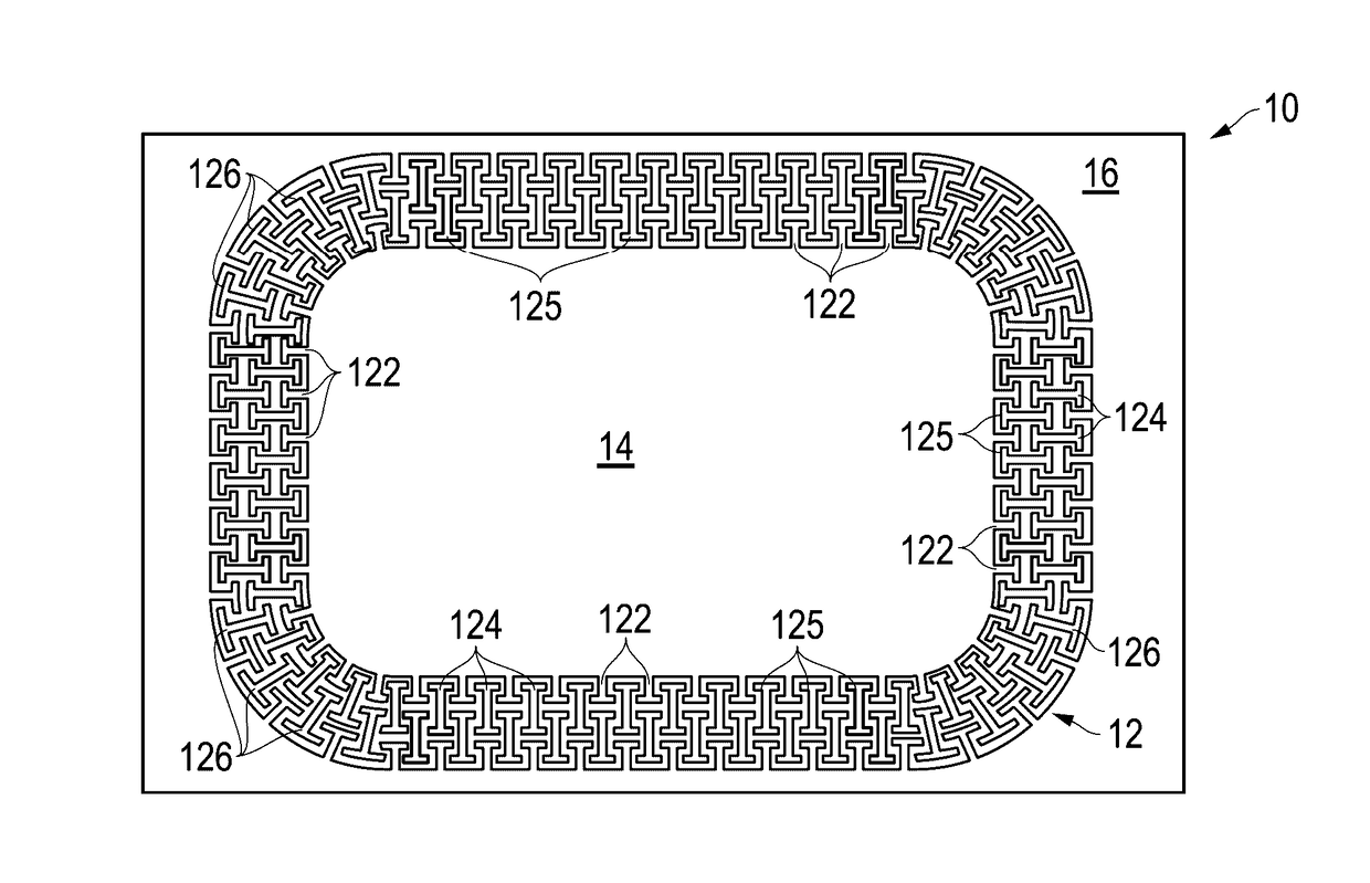
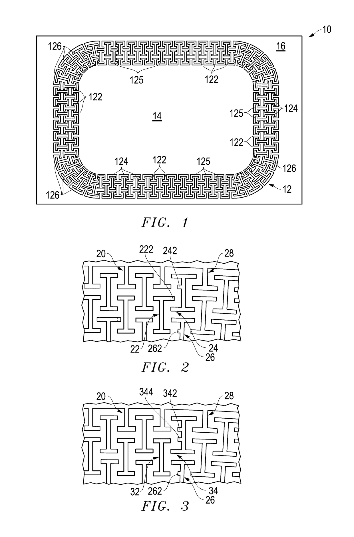
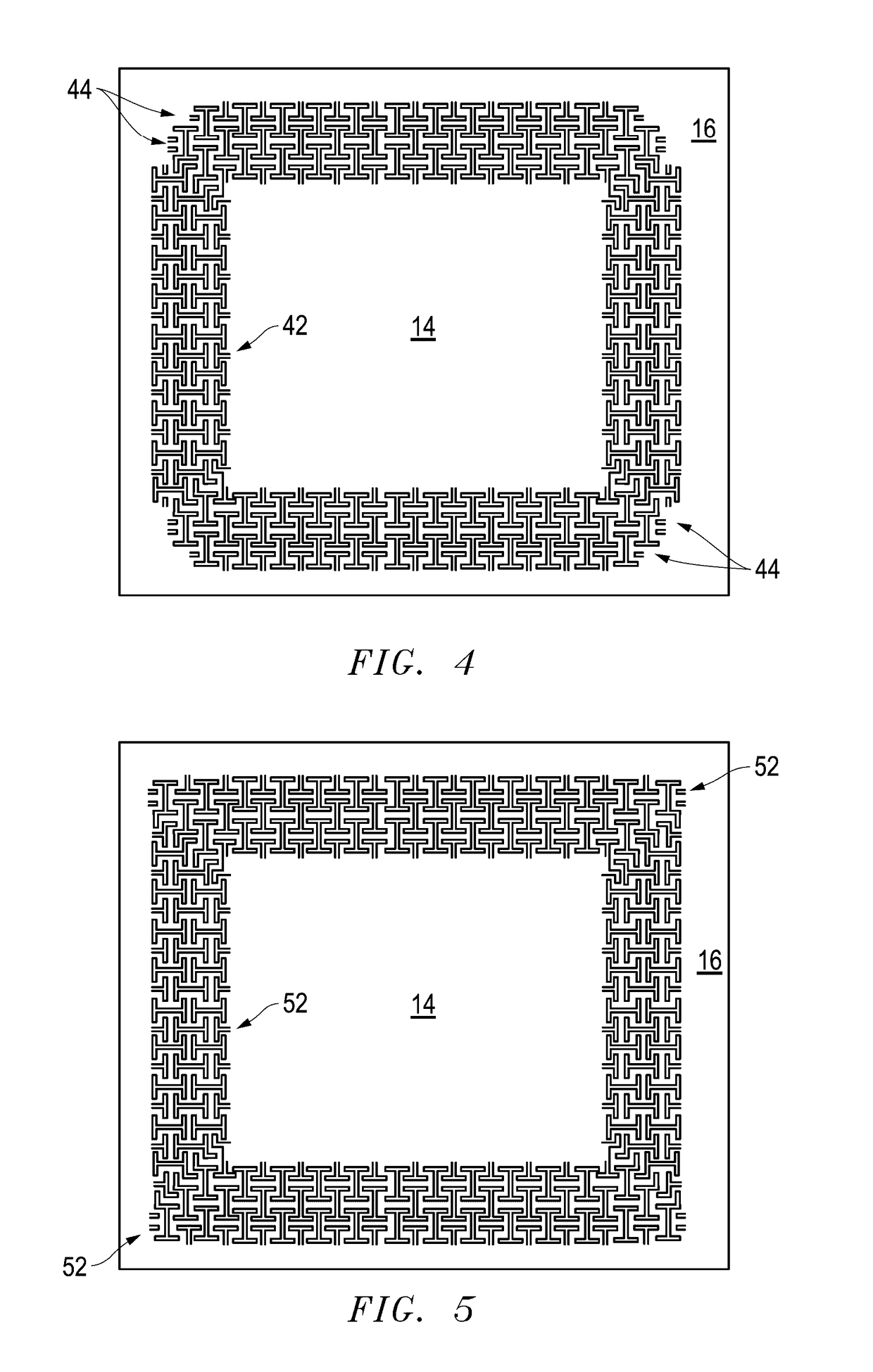
[0091]The electronic device of Embodiment 1, wherein the insulating structure has first and second opposing sides, wherein the first side includes the first anchor, and the second side does not include an anchor.
embodiment 3
[0092]The electronic device of Embodiment 1, wherein the first anchor is the portion of the substrate and has a first conductivity type; and the substrate includes a body portion and an adjacent portion from which the first anchor extends, wherein the adjacent portion has the first conductivity type is disposed between the body portion and the first anchor, and the body portion has a second conductivity type opposite the first conductivity type.
embodiment 4
[0093]The electronic device of Embodiment 1, wherein:[0094]the substrate includes a first body portion, a second body portion, and a second anchor;[0095]the insulating structure has first and second opposing sides;[0096]the first anchor extends from the first body portion of the substrate and lies along the first side of the insulating structure; and[0097]the second anchor extends from the second body portion of the substrate and lies along the second side of the insulating structure.
PUM
 Abstract
Description
Claims
Application Information