

Electronic device including a conductive structure surrounded by an insulating structure and a process for forming the same
a technology of insulating structure and conductive structure, which is applied in the direction of semiconductor devices, inductances, electrical apparatus, etc., can solve the problems of limiting the flexibility of electronic device design, large amount of insulating material, and limiting equipment throughpu
Active Publication Date: 2017-03-23
SEMICON COMPONENTS IND LLC
View PDF2 Cites 2 Cited by
- Summary
- Abstract
- Description
- Claims
- Application Information
AI Technical Summary
Benefits of technology
The patent text discusses the use of isolation structures in electronic devices to control high electrical fields. These structures can limit the flexibility in design and require a large amount of insulating material to be deposited, which can limit equipment throughput. The technical effects of the patent are to improve electronic devices and flexibility in designs while also increasing equipment throughput.
Problems solved by technology
The alternating regions can limit the flexibility in the design of the electronic device.
The large isolation region may require a large amount of insulating material to be deposited and limit equipment throughput.
Method used
View moreImage
Smart ImageViewing Examples

Examples
embodiment 1
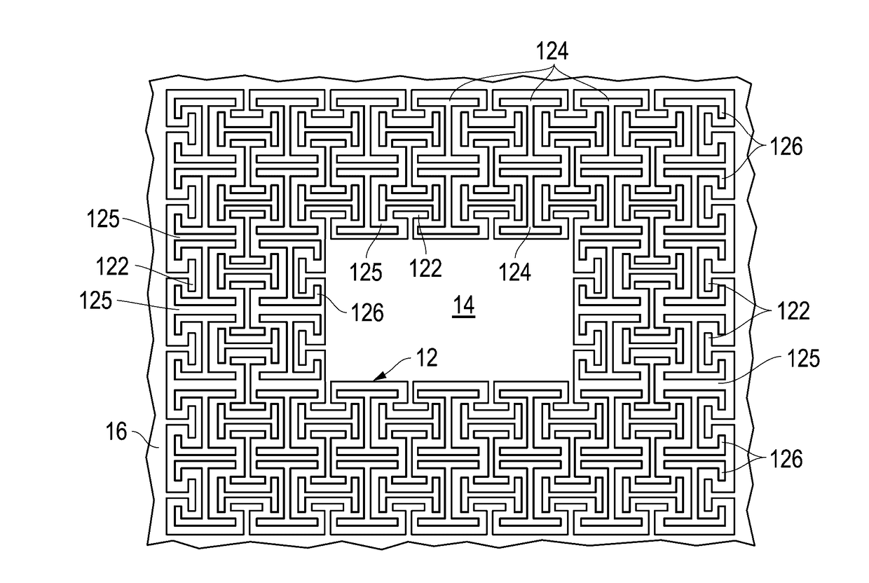
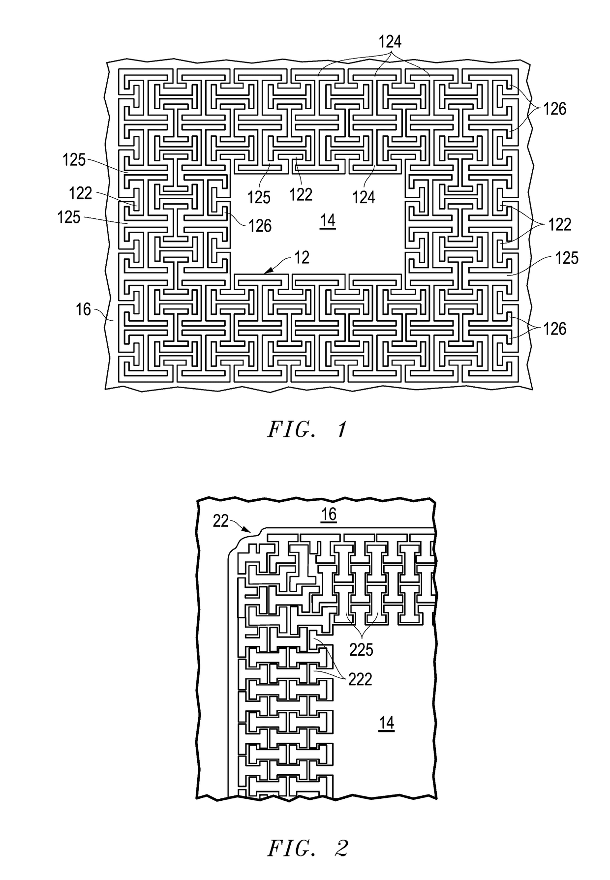
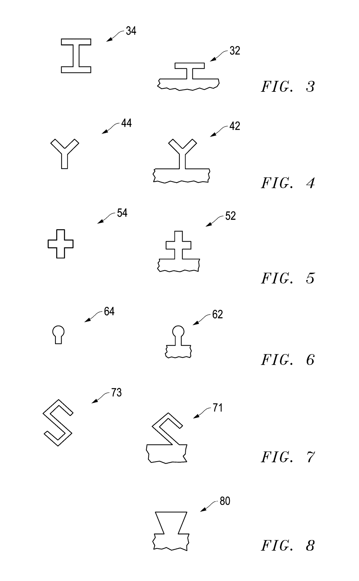
[0072]An electronic device can include a substrate; an insulating structure that is laterally surrounded by the substrate; and a first conductive structure or an active region that is laterally surrounded by the insulating structure and the substrate, wherein the first conductive structure or active region is laterally spaced apart from the substrate by at least 4 microns.
embodiment 2
[0073]The electronic device of Embodiment 1, further including a plurality of insulating pillars embedded within the first conductive structure.
embodiment 3
[0074]The electronic device of Embodiment 1, further including a second conductive structure, wherein the electronic device includes the first conductive structure that is laterally surrounded by the second conductive structure.
Login to View More PUM
 Abstract
An electronic device can include a substrate and an insulating structure laterally surrounded by the substrate. In an aspect, the electronic device can include a first conductive structure or an active region that is laterally surrounded by the insulating structure and the substrate. In another aspect, the electronic device can include an inductor surrounded by the insulating structure. In a further aspect, a process of forming an electronic device can include patterning a substrate to define a trench and a plurality of features, including a first feature and a second feature, within the trench; forming a first insulating layer within the trench; removing the first feature to create a first cavity; forming a second insulating layer to at least partly fill the first cavity; removing the second feature to create a second cavity; and forming a conductive or semiconductor structure within the second cavity.
Description
CROSS-REFERENCE TO RELATED APPLICATION[0001]This application claims priority under 35 U.S.C. § 119(e) to U.S. patent application Ser. No. 62 / 219,779 entitled “Deep Trench Isolation Devices and Methods,” by Grivna et al., filed Sep. 17, 2015, which is assigned to the current assignee hereof and incorporated herein by reference in its entirety.FIELD OF THE DISCLOSURE[0002]The present disclosure relates to electronic devices including insulating structures and processes of forming such electronic devices.RELATED ART[0003]Isolation structures are used to control high electrical fields that can be present within the die. The isolation structures can include alternating n-type and p-type regions, insulating layers, or a combination thereof. The alternating regions can limit the flexibility in the design of the electronic device. In another embodiment, a large isolation region can be formed using two insulating layers and a single mask. The large isolation region may require a large amount...
Claims
Login to View More Application Information
Patent Timeline
 Patent Type & AuthorityApplications(United States)
IPC IPC(8): H01L29/40H01L49/02
CPCH01L29/407H01L29/401H01L28/10H01L29/408H01L29/7811H01L29/7813H01L21/764H01L29/0649H01L29/0692H01L21/76232
InventorGRIVNA, GORDON M.
OwnerSEMICON COMPONENTS IND LLC