

Goa circuits and liquid crystal devices
a liquid crystal device and circuit technology, applied in the direction of instruments, static indicating devices, etc., can solve the problems of circuit invalidity, stv signal line blowout, stv signal line may reach a great level, etc., to reduce the load on the signal line, increase the current, and reduce the effect of driving capability
- Summary
- Abstract
- Description
- Claims
- Application Information
AI Technical Summary
Benefits of technology
Problems solved by technology
Method used
Image

Examples
first embodiment
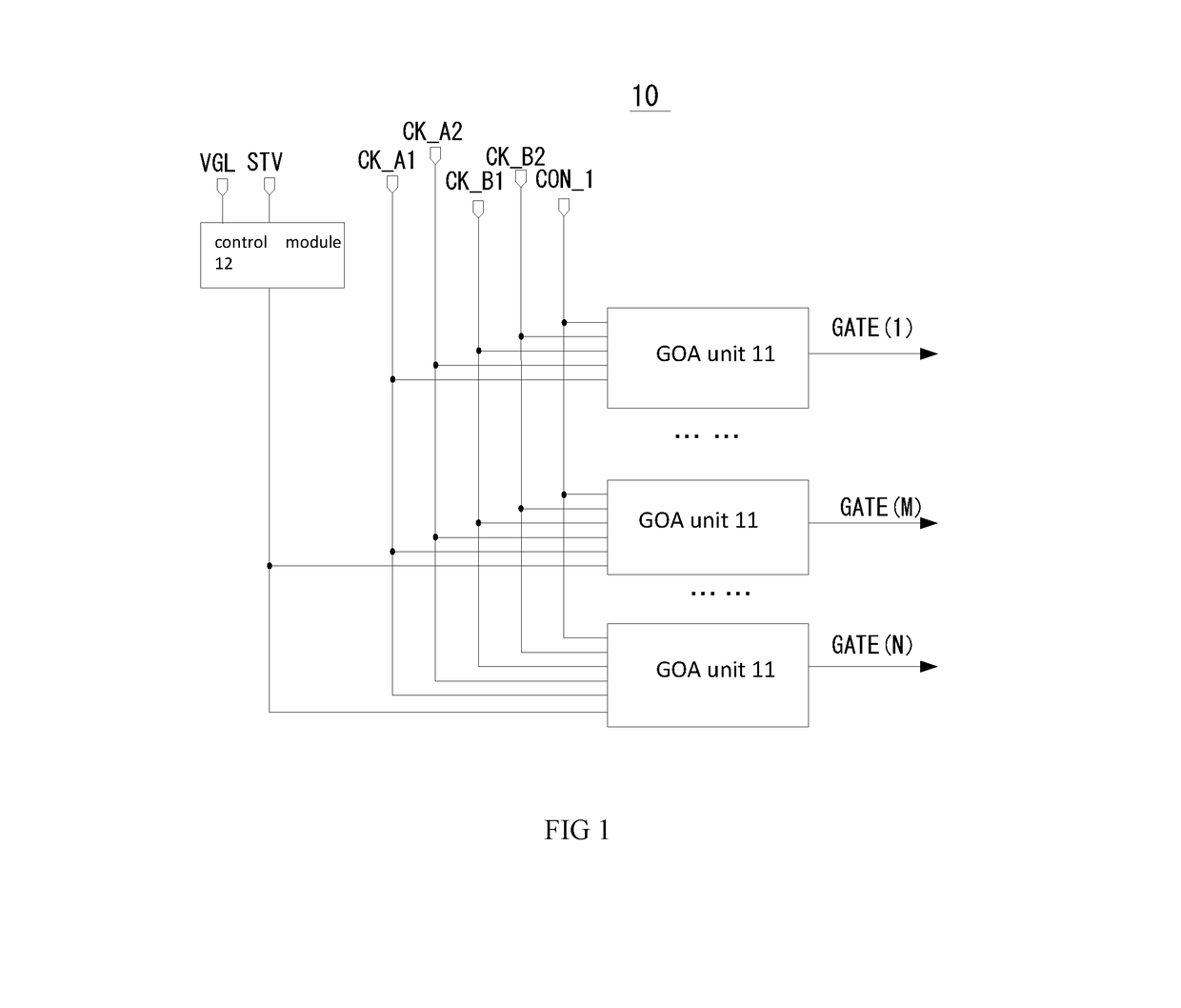
[0038]FIG. 1 is a schematic view of the GOA circuit in accordance with a As shown in FIG. 1, the GOA circuit 10 includes a plurality of cascaded GOA units 11 and a control module 12.
[0039]Each of the cascaded GOA units 11 is configured for charging corresponding horizontal scanning line within a display area when being driven by a first level clock (CK_A1), a second level clock (CK_A2), a first control clock (CK_B1), and a second control clock (CK_B2). The first level clock (CK_A1) and the second level clock (CK_A2) are configured for controlling an input of level signals (CON_1) of the GOA unit 11 and for controlling the generation of the gate driving signals GATE (N), wherein N is a natural number. The first control clock (CK_B1) and the second control clock (CK_B2) are configured for controlling the gate driving signals GATE (N) to be at a first level, i.e., an invalid level. The level signals (CON_1) may be turn-on pulse signals or the gate driving signals of adjacent GOA units...
second embodiment
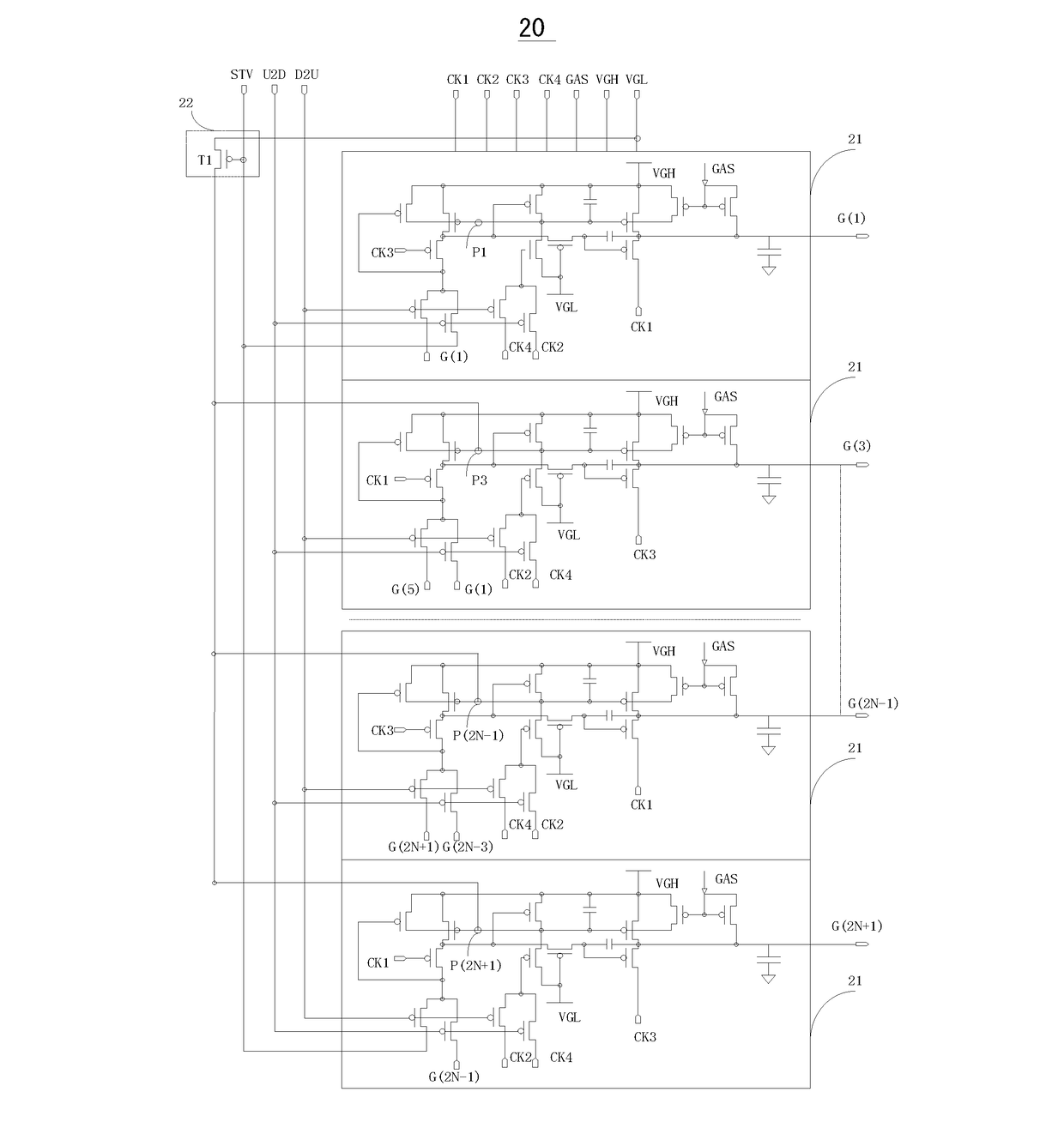
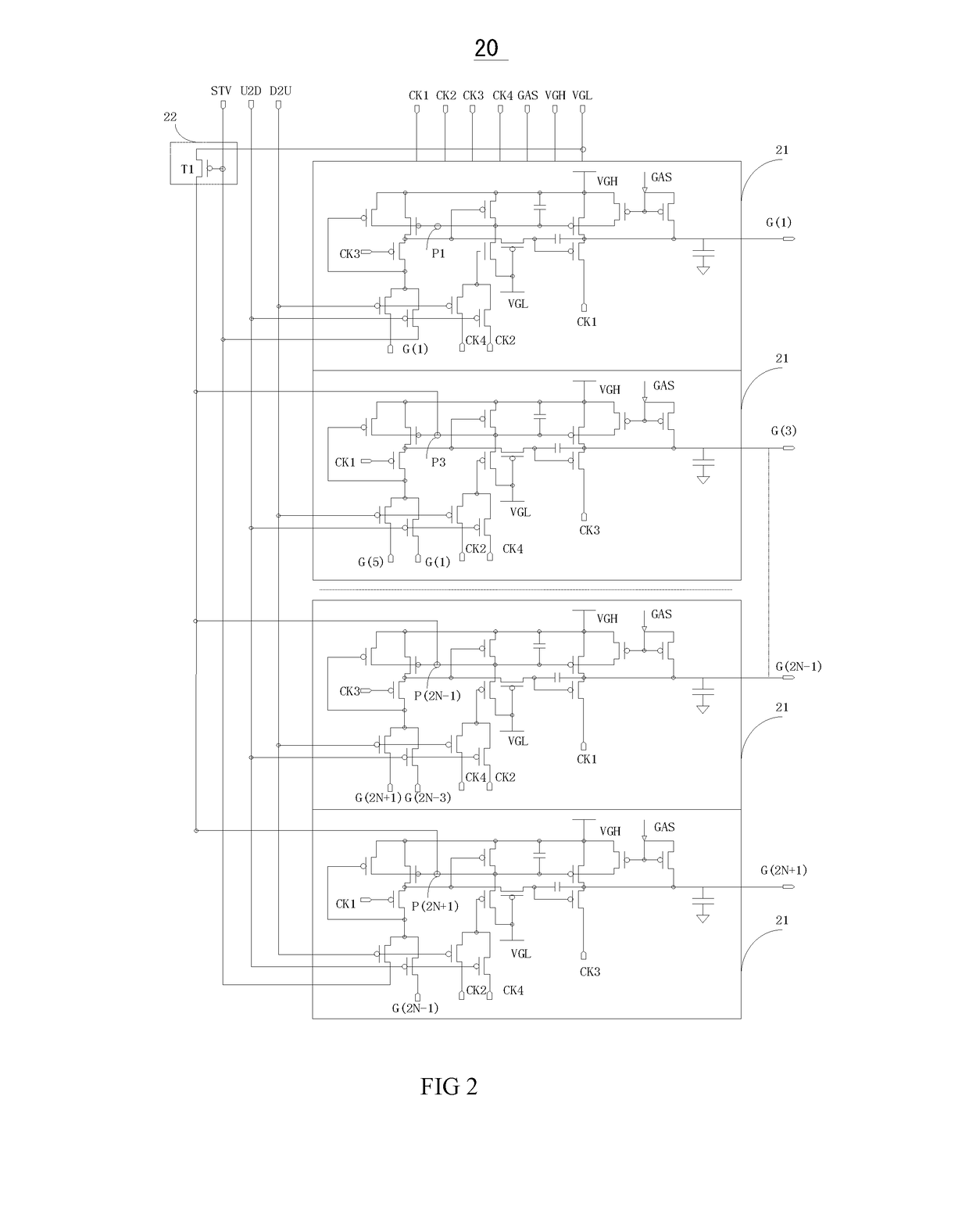
[0041]FIG. 2 is a schematic view of the GOA circuit in accordance with a In this embodiment, the GOA circuit is formed by GOA units at odd levels, and the GOA circuit is a PMOS circuit. As shown in FIG. 2, the GOA circuit 20 includes the GOA units at odd levels 21 and a control module 22.
[0042]The GOA circuit 20 includes the cascaded GOA units at odd levels 21. That is, the GOA circuit 20 includes the GOA units 21 at the first, the third, the fifth, and the (2N+1)-th level, and the GOA units 21 are cascaded.
[0043]The GOA circuit 20 receives the first clock signals (CK1), the second clock signals (CK2), the third clock signals (CK3), and the fourth clock signals (CK4). The first clock signals (CK1), the second clock signals (CK2), the third clock signals (CK3), and the fourth clock signals (CK4) are respectively valid within one clock period in sequence.
[0044]FIG. 3 is a circuit diagram of the GOA unit of the GOA circuit of FIG. 2. The GOA unit 21 includes a forward-backward scannin...
PUM
 Abstract
Description
Claims
Application Information