Device for connecting at least one nano-object associated with a chip enabling a connection to at least one external electrical system and method of fabrication thereof

a technology of at least one chip and a nano-object, applied in the direction of electrical apparatus, semiconductor devices, semiconductor/solid-state device details, etc., can solve the problem of fragile remaining portion

Active Publication Date: 2017-04-06
COMMISSARIAT A LENERGIE ATOMIQUE ET AUX ENERGIES ALTERNATIVES
View PDF6 Cites 4 Cited by
  • Summary
  • Abstract
  • Description
  • Claims
  • Application Information

AI Technical Summary

Benefits of technology

The patent describes a new way of assembling semiconductor devices that allows for smaller size and better sensitivity for electrical measurements on nano-objects. The method includes attaching a chip to a support material, removing a dummy block, and forming an insulating wall around the chip. The removal of the dummy block allows for easier access to the chip's conducting areas without damaging it, while the insulating wall provides protection and electrical insulation. The use of a dummy block also improves the cohesion of the chip and support material assembly. Overall, this method allows for smaller devices with improved sensitivity, while still providing protection and insulation.

Problems solved by technology

This remaining portion may prove to be fragile.
The problem is posed of producing a novel device for connecting a nano-object as well as a novel method for producing such a device.

Method used


Image

  • Device for connecting at least one nano-object associated with a chip enabling a connection to at least one external electrical system and method of fabrication thereof
  • Device for connecting at least one nano-object associated with a chip enabling a connection to at least one external electrical system and method of fabrication thereof
  • Device for connecting at least one nano-object associated with a chip enabling a connection to at least one external electrical system and method of fabrication thereof

Examples


Embodiment Construction

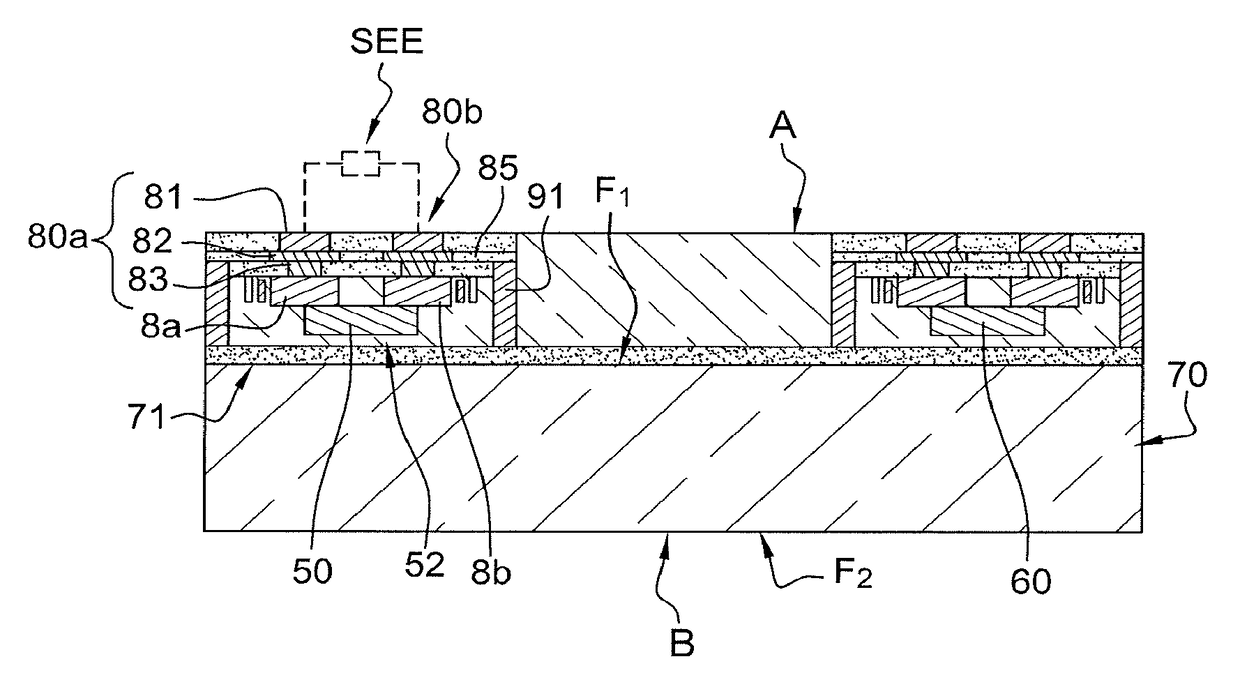
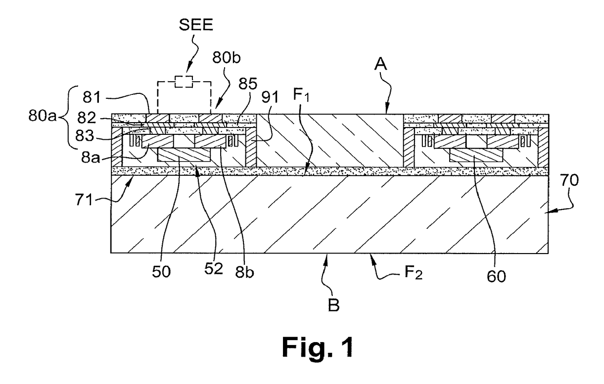
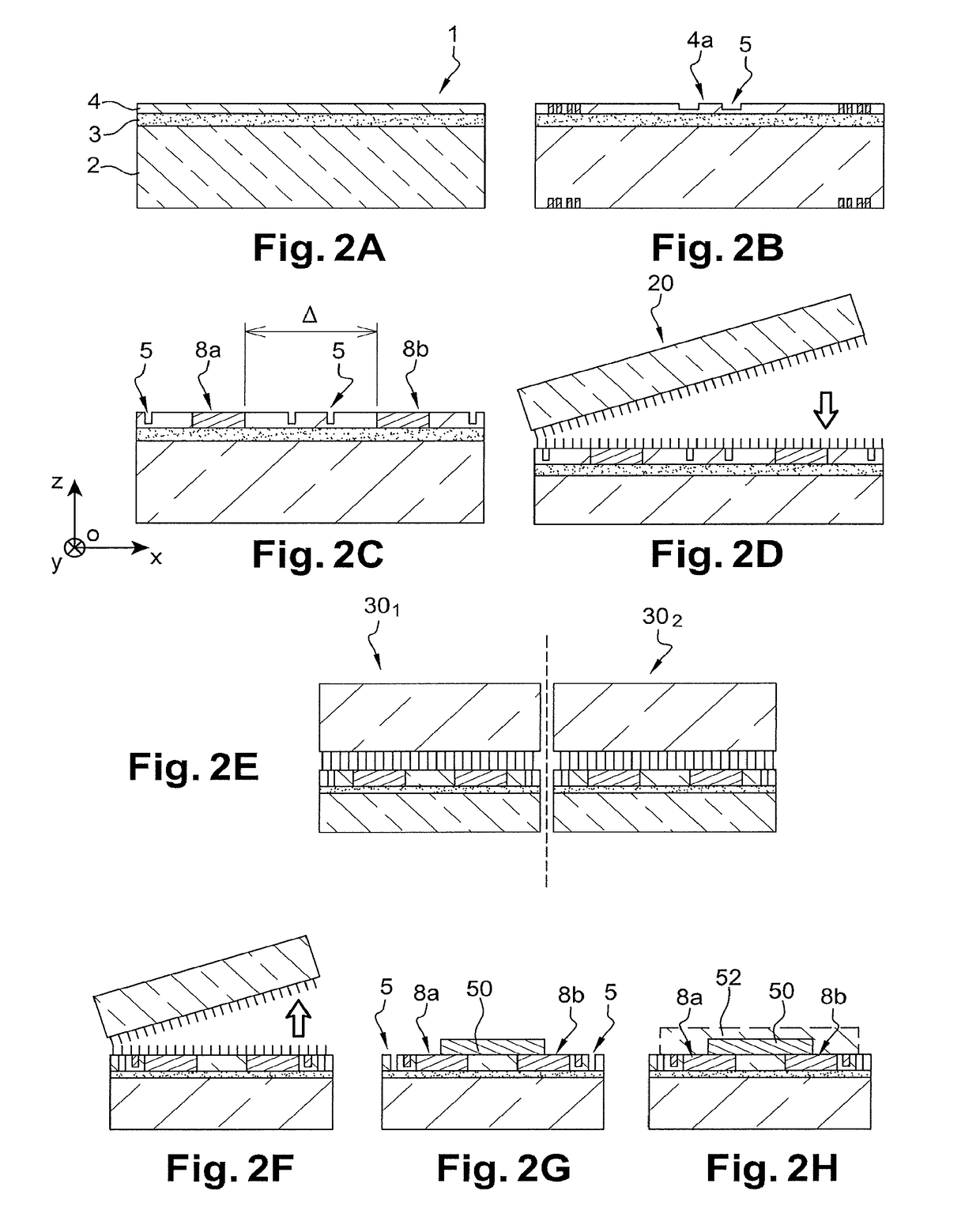
[0009]An embodiment of the present invention provides for a device for connecting at least one nano-object to an external electrical system, the device including: at least one first chip provided with one or more conducting areas and at least one first nano-object connected to a first conducting area and to a second conducting area among said conducting areas, the first chip being assembled on a support such that the first nano-object is arranged facing an upper face of the support, the device being further provided with connection elements capable of being connected to the external electrical system and arranged respectively on and in contact with the first conducting areas and with the second conducting area, the first connection elements being formed on the side of the upper face of the support and being accessible on the side of the upper face of the support.

[0010]A face called “first face” of the first chip on which the nano-object is situated is arranged facing the upper face ...


PUM


Abstract

Production of a device for connecting a nano-object to an external electrical system (SEE) including:a first chip provided with conducting areas (8a, 8b) and a first nano-object (50) connected to the conducting areas, the first chip being assembled on a support (70) such that the first nano-object is arranged facing an upper face of the support, the device being further provided with first connection elements (80a, 80b) capable of being connected to the external electrical system and arranged on and in contact with the first conducting areas (8a, 8b), the first connection elements being formed on the side of the upper face of the support (70) and being accessible from the side of the upper face of the support.

Description

TECHNICAL FIELD AND PRIOR ART[0001]The present invention relates to a device for connecting nano-objects to at least one external electrical system as well as a method for manufacturing such a device.[0002]“Nano-objects” is taken to mean objects of which at least one of the dimensions lies in the interval ranging from 0.1 nm to 1000 nm and more particularly from 1 nm to 100 nm, and included in this category of nano-objects are notably nanoparticles (organic or inorganic), nano-wires, molecules or associations of molecules, notably biological molecules such as viruses and bacteria.[0003]It is today sought to characterize smaller and smaller nano-objects or to manufacture structures at the nanometric scale. It is thus necessary to manufacture a device making it possible to measure electrically these nano-objects and to be able to connect them to an external electrical system configured to carry out an electrical test of nano-objects.[0004]The document US 2012 / 0161333 A1 provides for a...

Claims


Application Information

Patent Timeline
IPC IPC(8): H01L25/00H01L27/28H01L23/498H01L25/11H01L23/538
CPCH01L25/50H01L25/115H01L23/5389H01L29/0665H01L27/286H01L51/0098H01L23/49844B81B7/007B81B2207/07H01L25/165H01L25/162B81B2207/096B81B2207/097H10K19/20H10K30/671
Inventor THUAIRE, AURELIEREYNAUD, PATRICKLEDUC, PATRICKROLLAND, EMMANUEL
Owner COMMISSARIAT A LENERGIE ATOMIQUE ET AUX ENERGIES ALTERNATIVES
Why Eureka
Try Eureka