Fin-type field effect transistor and method of forming the same

a field effect transistor and transistor technology, applied in the field of semiconductor structure, can solve problems such as the degradation of the performance of the fin

Active Publication Date: 2017-04-06
UNITED MICROELECTRONICS CORP
View PDF6 Cites 8 Cited by
  • Summary
  • Abstract
  • Description
  • Claims
  • Application Information

AI Technical Summary

Benefits of technology

[0004]Accordingly, the present invention provides a FinFET and a method of forming the same, in which the lattice mismatch or dislocation issue of the conventional fin can be successfully resolved.

Problems solved by technology

However, the conventional silicon germanium fin is grown on a silicon substrate, so the lattice mismatch or dislocation occurs therebetween and the FinFET performance is therefore degraded.

Method used


Image

  • Fin-type field effect transistor and method of forming the same
  • Fin-type field effect transistor and method of forming the same
  • Fin-type field effect transistor and method of forming the same

Examples


Embodiment Construction

[0030]Reference will now be made in detail to the present preferred embodiments of the invention, examples of which are illustrated in the accompanying drawings. Wherever possible, the same reference numbers are used in the drawings and the description to refer to the same or like parts.

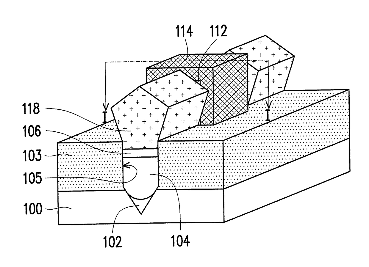
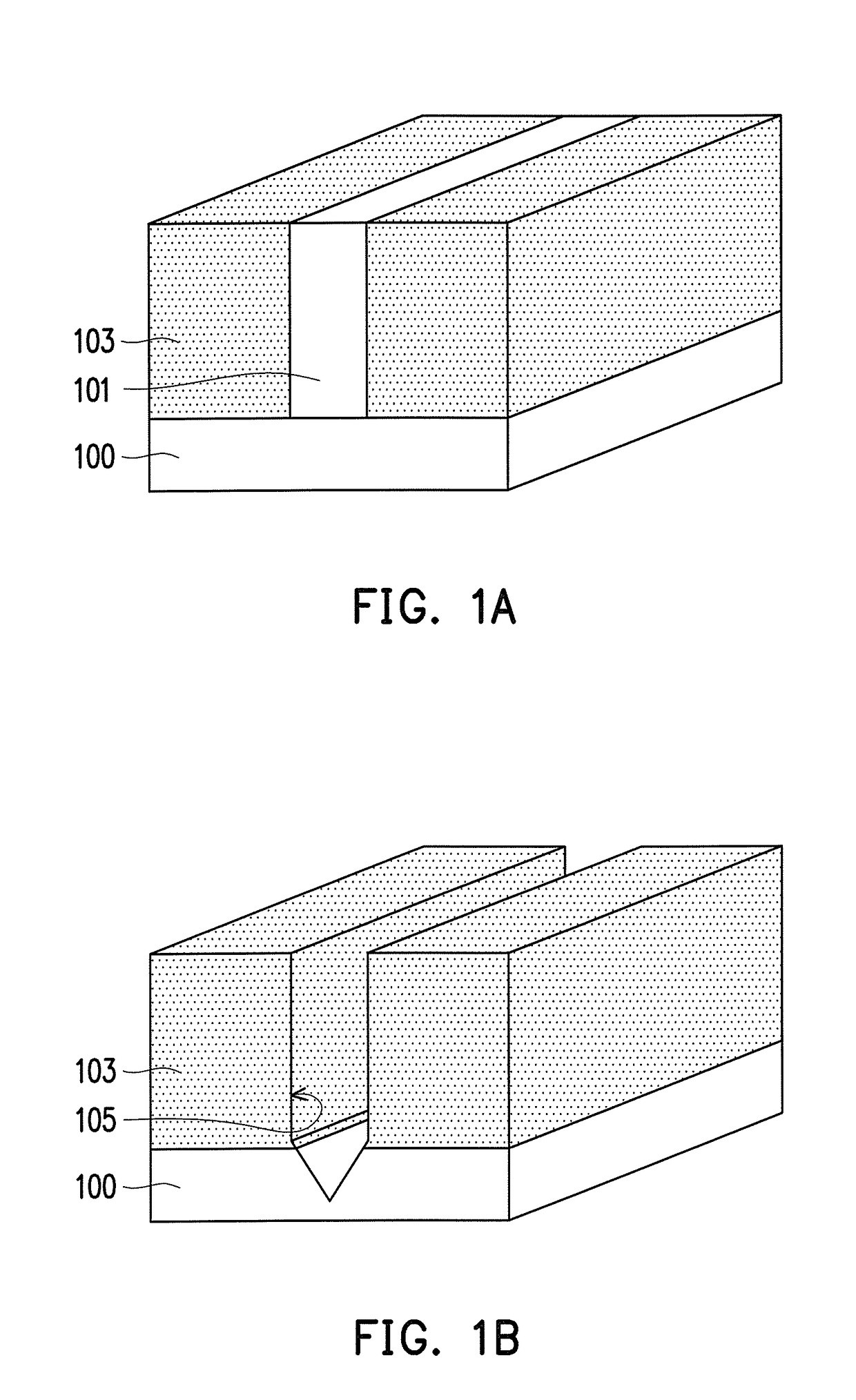
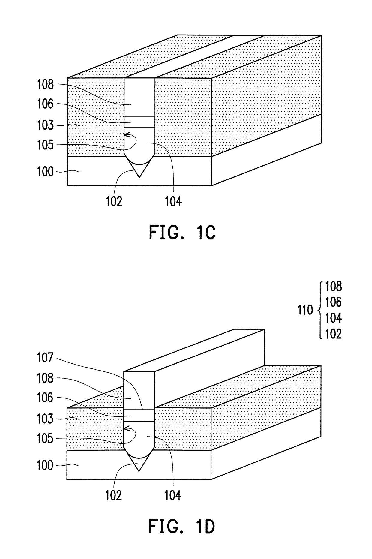
[0031]FIG. 1A to FIG. 1E are schematic perspective views of a method of forming a FinFET according to an embodiment of the present invention. FIG. 2 is a schematic cross-sectional view taken along line I-I of FIG. 1E.

[0032]Referring to FIG. 1A, a substrate 100 with at least one dummy fin 101 is provided. The substrate 100 can be a semiconductor substrate, and the dummy fin 101 can be a semiconductor fin. In an embodiment, the substrate 100 and the dummy fin 101 are made by the same material. For example, the dummy fin 101 and the substrate 100 are made by silicon, but the present invention is not limited thereto. In an embodiment, the method of forming the substrate 100 with the dummy fin 101 include...


PUM


Abstract

Provided is a FinFET including a substrate, at least one fin and at least one gate. A portion of the at least one fin is embedded in the substrate. The at least one fin includes, from bottom to top, a seed layer, a stress relaxation layer and a channel layer. The at least one gate is across the at least one fin. A method of forming a FinFET is further provided.

Description

CROSS-REFERENCE TO RELATED APPLICATION[0001]This application claims the priority benefit of Taiwan application serial no. 104132649, filed on Oct. 2, 2015. The entirety of the above-mentioned patent application is hereby incorporated by reference herein and made a part of this specification.FIELD OF THE PRESENT INVENTION[0002]The present invention is related to a semiconductor structure and a method of forming the same, and more generally to a fin-type field effect transistor (FinFET) and a method of forming the same.DESCRIPTION OF RELATED ART[0003]FinFET devices are developed as the dimensions of integrated circuits are shrunk and the demands for transistors with higher driving currents and smaller sizes are increased. The channel of a FinFET is formed on the top and side surfaces of each fin, so the FinFET is provided with a greater channel length, and the driving current is therefore improved. However, the conventional silicon germanium fin is grown on a silicon substrate, so the...

Claims


Application Information

Patent Timeline
Patent Type & Authority Applications(United States)
IPC IPC(8): H01L29/06H01L21/768H01L29/66H01L21/225H01L29/78H01L29/10
CPCH01L29/0615H01L29/785H01L29/1033H01L21/76802H01L21/2253H01L21/76871H01L29/66795H01L29/1054
Inventor CHIANG, HUAI-TZULIN, SHENG-HAOLEE, HAO-MINGYANG, YU-RUHUANG, SHIH-HSIENCHEN, CHIEN-HUNGWU, CHUN-YUANTSAI, CHENG-TZUNG
Owner UNITED MICROELECTRONICS CORP
Why Eureka
Try Eureka