Pixel circuit, display panel and display device comprising the pixel circuit

a pixel circuit and display panel technology, applied in the field of display devices, can solve the problems of non-uniform image quality in a plurality of pixel regions, inability to use oled display devices driven through progressive emission mode, and inability to solve the above-mentioned problems, and achieve the effect of prolonging the lifetime of the circui

Active Publication Date: 2017-04-20
SHENZHEN CHINA STAR OPTOELECTRONICS TECH CO LTD
View PDF7 Cites 19 Cited by
  • Summary
  • Abstract
  • Description
  • Claims
  • Application Information

AI Technical Summary

Benefits of technology

[0010]One of the technical problems to be solved by the present disclosure is to provide a pixel circuit, which can solve the problem of the drifting of the threshold voltage and thus prolo

Problems solved by technology

Due to the instable power of the laser beam, the Thin Film Transistors formed in the scanning lines obtained by the scanning of the laser beam may have different threshold voltages, and thus the problem of non-uniform image qualities in a plurality of pixel regions could be caused.
However, in the above pixel circuit, since the Thin Film Transistor T2 is under the state of positive bias driving for a long time,

Method used


Image

  • Pixel circuit, display panel and display device comprising the pixel circuit
  • Pixel circuit, display panel and display device comprising the pixel circuit
  • Pixel circuit, display panel and display device comprising the pixel circuit

Examples


Embodiment Construction

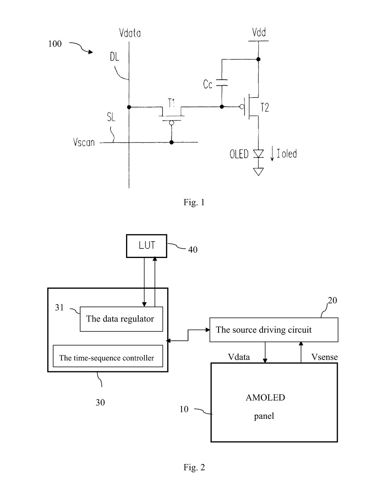
[0036]The present disclosure will be illustrated in detail hereinafter in combination with the accompanying drawings to make the purpose, technical solutions, and advantages of the present disclosure more clear.

[0037]It should be noted that, in the embodiments of the present disclosure, when a component, such as a substrate, layer, region, thin film, or electrode, is arranged on the “upper” or “lower” side of another component, it can be arranged on the upper or lower side of another component directly, or can be arranged on the upper or lower side of another component indirectly with a spacer component arranged therebetween. In addition, the size and thickness of the components in the accompanying drawings can be enlarged, omitted, or simplified for the purpose of clarity and convenient for explanation. Moreover, the size of the components as shown in the accompanying drawings is not the actual size of the corresponding components.

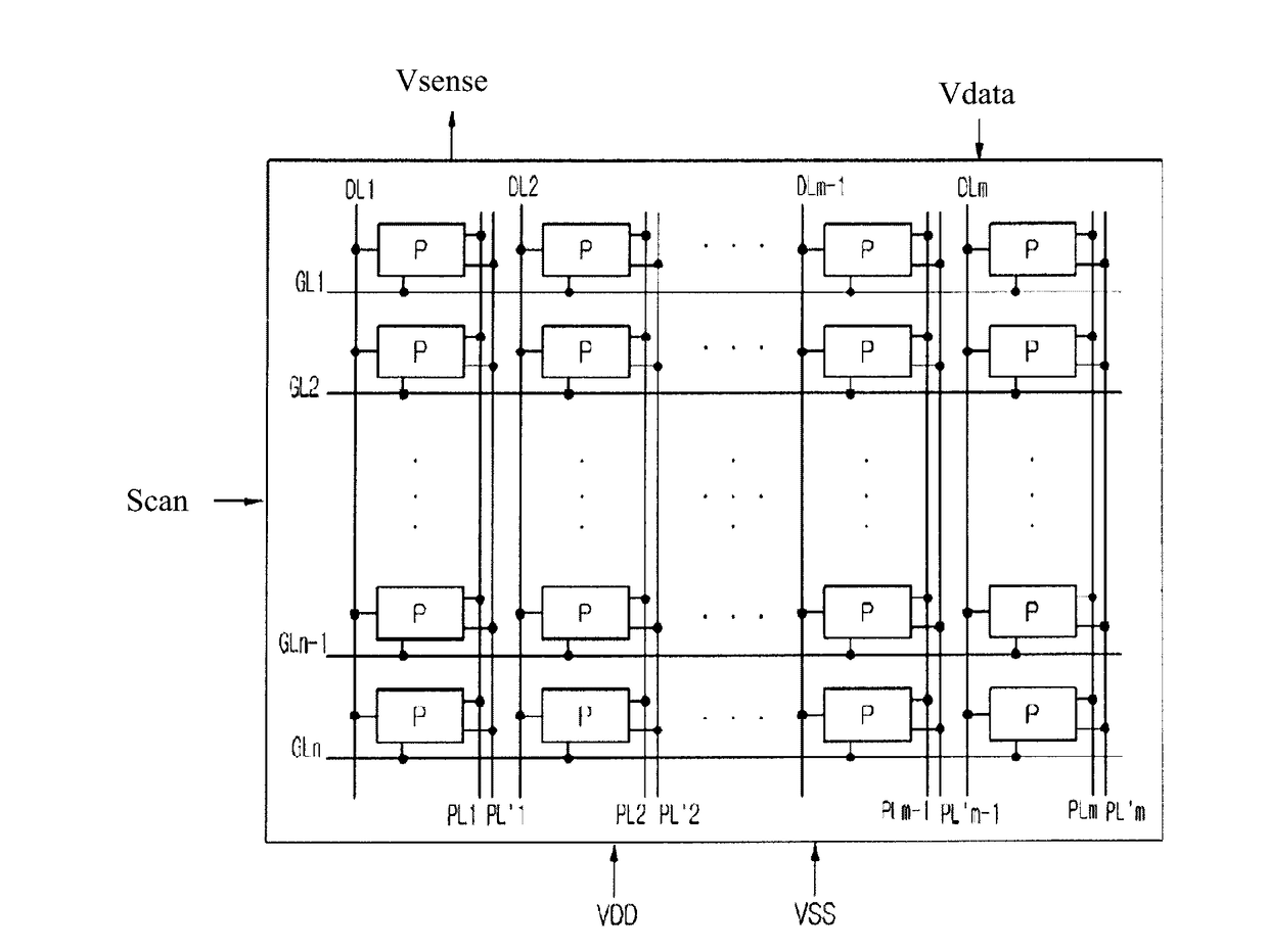
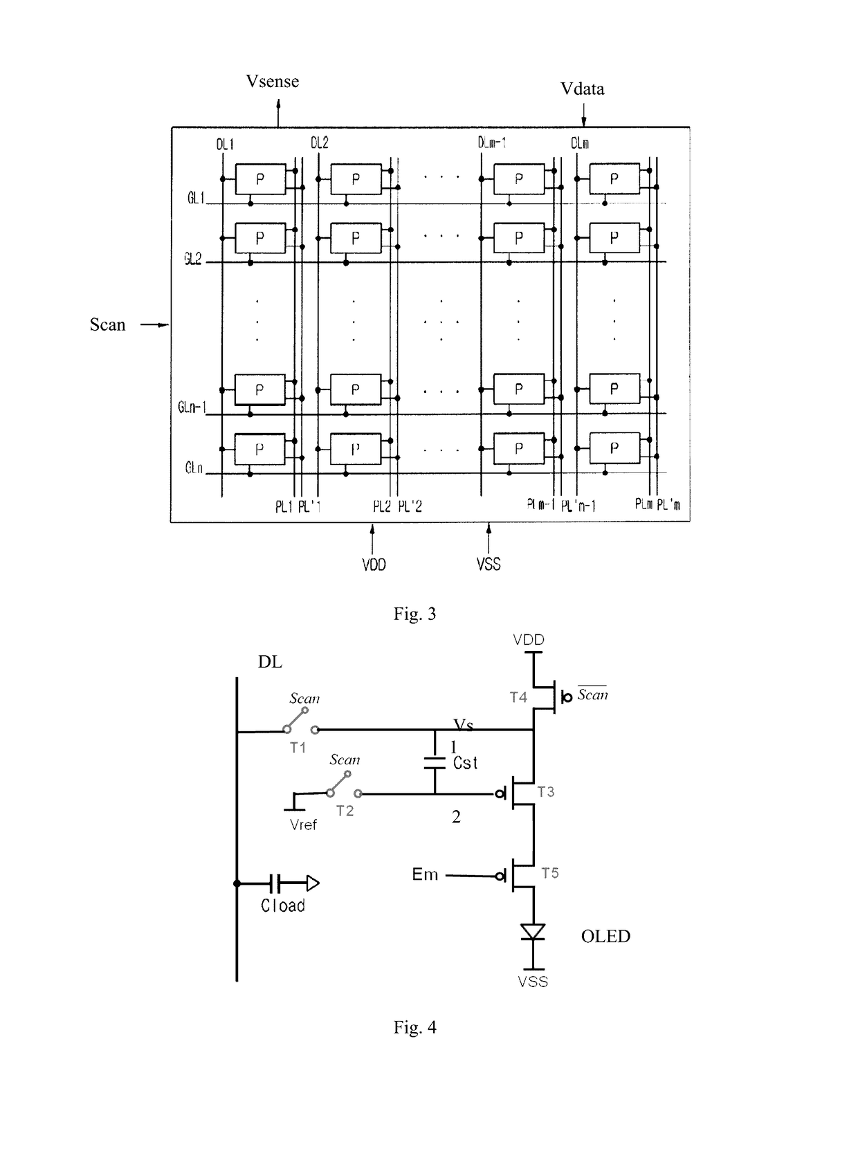
[0038]FIG. 2 schematically shows a structure of an ...


PUM


Abstract

The present disclosure discloses a pixel circuit, a display panel comprising the pixel circuit, and a display device comprising the pixel circuit. The pixel circuit comprises a first transistor, a second transistor, a third transistor, a fourth transistor, and a fifth transistor. The lifetime of the circuit can be prolonged by the pixel circuit with threshold voltage compensation function of the present disclosure. The pixel circuit can not only be used in large sized display device driven through SE mode, but also be used in medium or small sized display device driven through PE mode.

Description

CROSS REFERENCE TO RELATED APPLICATION[0001]The present application claims benefit of Chinese patent application CN 201410321425.2, entitled “Pixel Circuit, Display Panel and Display Device Comprising the Pixel Circuit” and filed on Jul. 7, 2014, which is incorporated herein by reference.FIELD OF THE INVENTION[0002]The present disclosure relates to the technical field of display device, and particularly relates to Active Matrix Organic Light Emitting Diode (AMOLED) display. Specifically, the present disclosure relates to a pixel circuit, a display panel comprising the pixel circuit, and a display device comprising the pixel circuit.BACKGROUND OF THE INVENTION[0003]After Thin Film Transistor-Liquid Crystal Display (TFT-LCD) emerges, the AMOLED display panel has become a new generation display panel with the most promising future. Compared with traditional liquid crystal display panel, the AMOLED panel has the advantages of thin, light, and simple structure, self-luminous without back...

Claims


Application Information

Patent Timeline
IPC IPC(8): G09G3/3233G09G3/3266G09G3/3258
CPCG09G3/3233G09G3/3266G09G2300/0871G09G2320/0233G09G2310/0289G09G2320/0242G09G2300/0819G09G2300/0842G09G2300/0861G09G3/30G09G3/32
Inventor KUO, PING SHENG
Owner SHENZHEN CHINA STAR OPTOELECTRONICS TECH CO LTD
Why Eureka
Try Eureka