Chip package and manufacturing method thereof

Inactive Publication Date: 2017-04-20
XINTEC INC
View PDF0 Cites 0 Cited by
  • Summary
  • Abstract
  • Description
  • Claims
  • Application Information

AI Technical Summary

Benefits of technology

The present invention provides a chip package with a dam element and a height-increasing element, which helps to shield light and prevent interference during image sensing. Additionally, a light transmissive sheet can be used to increase the distance between the chip and the image sensing area, reducing flare.

Problems solved by technology

Therefore, when the image sensing area receives an image, a lens flare issue is prone to occur.
In the manufacturing processes of an image sensor, if there is no glass sheet disposed on a wafer which is not yet cut to form a plurality of chips, when the wafer is thin, it is difficult to remove the wafer which has a ball grid array due to process limitations.
Moreover, image sensing areas of the wafer may easily be contaminated during the manufacturing processes, such that it is difficult to improve the yield of the chip package.
As a result, when the image sensing area receives an image, a flare issue does not easily occur.

Method used


Image

  • Chip package and manufacturing method thereof
  • Chip package and manufacturing method thereof
  • Chip package and manufacturing method thereof

Examples


Embodiment Construction

[0029]Reference will now be made in detail to the present embodiments of the invention, examples of which are illustrated in the accompanying drawings. Wherever possible, the same reference numbers are used in the drawings and the description to refer to the same or like parts.

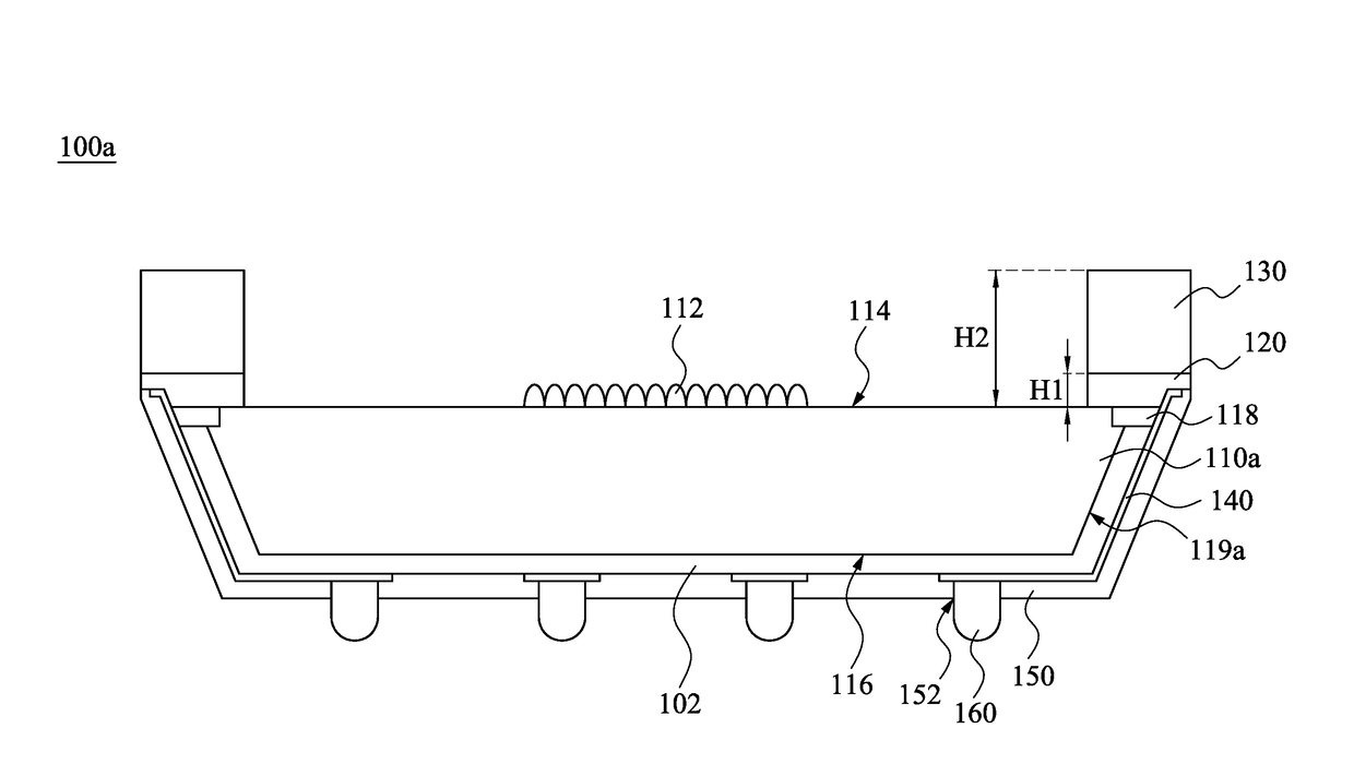
[0030]FIG. 1 is a cross-sectional view of a chip package 100a according to one embodiment of the present invention. As shown in FIG. 1, the chip package 100a includes a chip 110a, a dam element 120, and a height-increasing element 130. The chip 110a has an image sensing area 112, a first surface 114, and a second surface 116 that is opposite to the first surface 114. The image sensing area 112 is located on the first surface 114 of the chip 110a. The dam element 120 is located on the first surface 114 of the chip 110a and surrounds the image sensing area 112. The height-increasing element 130 is located on the dam element 120, such that the dam element 120 is present between the height-increasing element 130 a...


PUM


Abstract

A chip package includes a chip, a dam element, and a height-increasing element. The chip has an image sensing area, a first surface, and a second surface opposite to the first surface. The image sensing area is located on the first surface of the chip. The dam element is located on the first surface of the chip and surrounds the image sensing area. The height-increasing element is located on the dam element, such that the dam element is between the height-increasing element and the chip.

Description

RELATED APPLICATIONS[0001]This application claims priority to U.S. provisional Application Ser. No. 62 / 242,502, filed Oct. 16, 2015, which is herein incorporated by reference.BACKGROUND[0002]Field of Invention[0003]The present invention relates to a chip package and a manufacturing method of the chip package.[0004]Description of Related Art[0005]In manufacturing a chip package (e.g., a CMOS chip) of an image sensor, a glass sheet is often used to cover a surface of a chip, thereby protecting an image sensing area of the chip. In a typical chip package having a glass sheet, the thickness of a dam element that is disposed between the chip and the glass sheet is the same as a distance between the glass sheet and the chip, such as about in a range from 40 μm to 45 μm. Therefore, when the image sensing area receives an image, a lens flare issue is prone to occur.[0006]In the manufacturing processes of an image sensor, if there is no glass sheet disposed on a wafer which is not yet cut to...

Claims


Application Information

Patent Timeline
IPC IPC(8): H01L27/146H01L21/56H01L23/00
CPCH01L27/14618H01L24/08H01L2224/0231H01L21/563H01L2224/0237H01L24/03H01L27/146H01L27/14601H01L27/14683H01L2224/13101H01L24/13H01L2924/16235H01L23/481H01L2924/014H01L2924/00014
Inventor WU, JYUN-LIANGLIN, CHIA-SHENGLEE, PO-HANHO, YEN-SHIH
Owner XINTEC INC
Why Eureka
Try Eureka