Fabrication method of semiconductor multilayer structure

a technology of semiconductors and fabrication methods, applied in the direction of semiconductor devices, basic electric elements, electrical equipment, etc., can solve the problems of high lattice mismatch, melt back etching, cracking of gan films, etc., to improve the quality and flatness of al contained nitride layers, reduce the temperature of growing al contained nitride buffer layers, and enhance the effect of al (al) migration

Inactive Publication Date: 2017-04-27
HERMES EPITEK
View PDF1 Cites 1 Cited by
  • Summary
  • Abstract
  • Description
  • Claims
  • Application Information

AI Technical Summary

Benefits of technology

[0007]The present invention is directed to a fabrication method of a semiconductor multilayer structure thereof. By utilizing the indium-containing and / or gallium-containing catalyst, the aluminum (Al) migration can be enhanced to increase quality and flatness of the Al contained nitride layer, the temperature of growing Al contained nitride buffer layer can be lowered and thermal defects can also be prevented. Additionally, the costs and energy consumption can be reduced.
[0008]According to one embodiment of the present invention, a fabrication method of a semiconductor multilayer structure comprising: providing a silicon substrate in a reaction chamber; and depositing a plurality of semiconductor layers on the silicon substrate, wherein at least one of the semiconductor layers is an aluminum contained nitride layer; and an indium-containing catalyst is introduced into the chamber to enhance migration of aluminum in the aluminum contained nitride layer during depositing the aluminum contained nitride layer.

Problems solved by technology

However, it has disadvantages including higher lattice mismatch with GaN (it causes crack of GaN films when lowering temperature) and melt back etching effect.
Nevertheless, higher temperature is required to grow the MN buffer layer; the equipment to grow GaN cannot satisfy the requirement.
This will increase costs to purchase additional equipment and energy consumption.

Method used


Image

  • Fabrication method of semiconductor multilayer structure
  • Fabrication method of semiconductor multilayer structure
  • Fabrication method of semiconductor multilayer structure

Examples


Embodiment Construction

[0017]The detailed explanation of the present invention is described as follows. The described preferred embodiments are presented for purposes of illustrations and description, and they are not intended to limit the scope of the present invention.

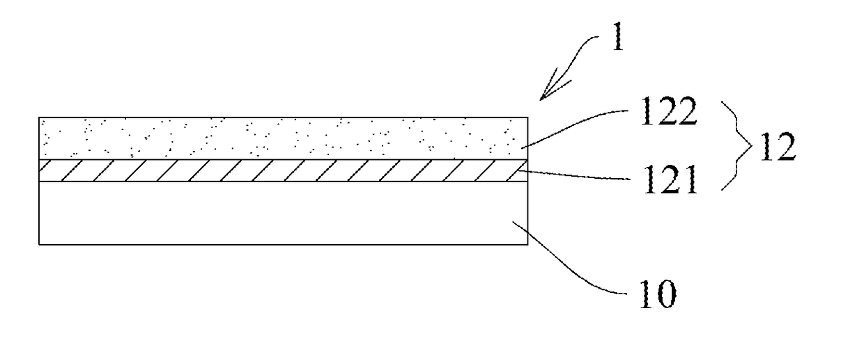
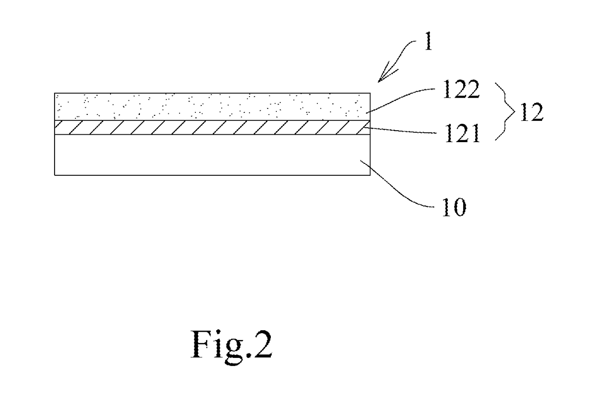
[0018]Referring to FIG. 1 and FIG. 2, wherein FIG. 1 is a flowchart illustrating the fabrication method of the semiconductor multilayer structure according to one embodiment of the present invention; and FIG. 2 is a schematic diagram illustrating the semiconductor multilayer structure according to one embodiment of the present invention. The fabrication method of a semiconductor multilayer structure 1 is described in the following. First, a silicon substrate 10 is provided in a reaction chamber (step S10). And then, a plurality of semiconductor layers 12 is deposited on the silicon substrate 10, wherein at least one of the semiconductor layers 20 is an aluminum contained nitride layer. An indium-containing catalyst is introduced into the c...


PUM

PropertyMeasurementUnit
concentrationaaaaaaaaaa
semiconductoraaaaaaaaaa
sizeaaaaaaaaaa

Abstract

The present invention is directed to a fabrication method of a semiconductor multilayer structure. By utilizing the indium-containing catalyst and / or gallium-containing catalyst, the aluminum migration can be enhanced to increase quality and flatness of the aluminum contained nitride buffer layer. Furthermore, the costs and energy consumption can be reduced too.

Description

BACKGROUND OF THE INVENTION[0001]1. FIELD OF THE INVENTION[0002]This is a Divisional Application of U.S. patent application Ser. No. 14 / 678,475, filed in Apr. 3, 2015, for which priority is claimed under 35 U.S.C. §120.[0003]The present invention relates to a semiconductor multilayer structure and fabrication method thereof, and more particularly to a semiconductor multilayer structure and fabrication method thereof for an optical device or an electronic device.[0004]2. DESCRIPTION OF THE PRIOR ART[0005]Currently, large size silicon wafers have become favored choice to fabricate light emitting diodes and high power devices. Comparing to sapphire substrate, the silicon substrate has advantages including: lower cost, better efficiency of heat dissipation and capability of larger size. However, it has disadvantages including higher lattice mismatch with GaN (it causes crack of GaN films when lowering temperature) and melt back etching effect. To overcome these drawbacks, AlN is usually...

Claims


Application Information

Patent Timeline
Patent Type & Authority Applications(United States)
IPC IPC(8): H01L21/02H01L29/20H01L29/205H01L29/15
CPCH01L21/0254H01L21/02381H01L21/02458H01L29/205H01L29/151H01L29/2003H01L21/02505H01L29/155H01L33/0075
Inventor KOBAYASHI, TAKASHILIN, PO-JUNGWU, CHIH-SHENGCHUNG, BU-CHIN
Owner HERMES EPITEK
Why Eureka
Try Eureka