
Functional yarn equipped with semiconductor functional elements

a functional element and functional yarn technology, applied in the direction of basic electric elements, semiconductor devices, electrical apparatus, etc., can solve the problems of ineffective inability to achieve effective utilization of beneficial aspects of functional yarns equipped with semiconductor functional elements, and inability to prevent electrical short circuits. , to achieve the effect of preventing electrical short circuits and facilitating electrical connections

Inactive Publication Date: 2017-05-11
SPHELAR POWER
View PDF2 Cites 2 Cited by
  • Summary
  • Abstract
  • Description
  • Claims
  • Application Information

AI Technical Summary

Benefits of technology

The present invention provides a functional yarn that can be easily connected electrically after being processed into a textile. The yarn has conducting wire portions that are not insulated, preventing electrical short circuiting and maintaining flexibility and expansion characteristics. A smaller line width of the conducting wire region in the electrically conductive direction also helps to maintain these characteristics. Overall, the invention provides a flexible and expandable functional yarn that is easy to use and maintains its characteristics after processing.

Problems solved by technology

However, with a construction like that of the functional yarn equipped with semiconductor functional elements of JP Patent 5,138,976 in which the plurality of semiconductor functional elements and the pair of conducting wires are completely covered with synthetic resin, when establishing electrical connection in series or in parallel partway along the conducting wire direction between one functional yarn equipped with semiconductor functional elements and another functional yarn equipped with semiconductor functional elements, since it is difficult to establish connection between the functional yarns equipped with semiconductor functional elements due to the impediment provided by the synthetic resin, accordingly it is not easy to perform adjustment of the generated current or the generated voltage, so that there is the problem that it is not possible to utilize the beneficial aspects of the functional yarn equipped with semiconductor functional elements in an effective manner.
Moreover, since the functional yarn equipped with semiconductor functional elements becomes thicker when the functional yarn equipped with semiconductor functional elements is completely covered with synthetic resin, accordingly its flexibility as a wire material is undesirably reduced.
Due to this, after the functional yarn equipped with semiconductor functional elements has been used as a weft and an insulating yarn has been used as the warp, for example, and these have been processed into a textile, the flexibility and the expansion characteristic of the manufactured textile are lost, which is undesirable.
In other words, there is the problem that, the more the amount of covering with synthetic resin upon the functional yarn equipped with semiconductor functional elements increases, the more difficult it becomes to realize its function as a normal yarn material.
Furthermore, if processing into a textile is performed in the state in which the functional yarn equipped with semiconductor functional elements is not covered with synthetic resin, then, as described above, there is the problem of undesirable short circuiting between conducting wire portions within the pair of conducting wires of the functional yarn equipped with semiconductor functional elements on which semiconductor functional elements are not arranged.

Method used

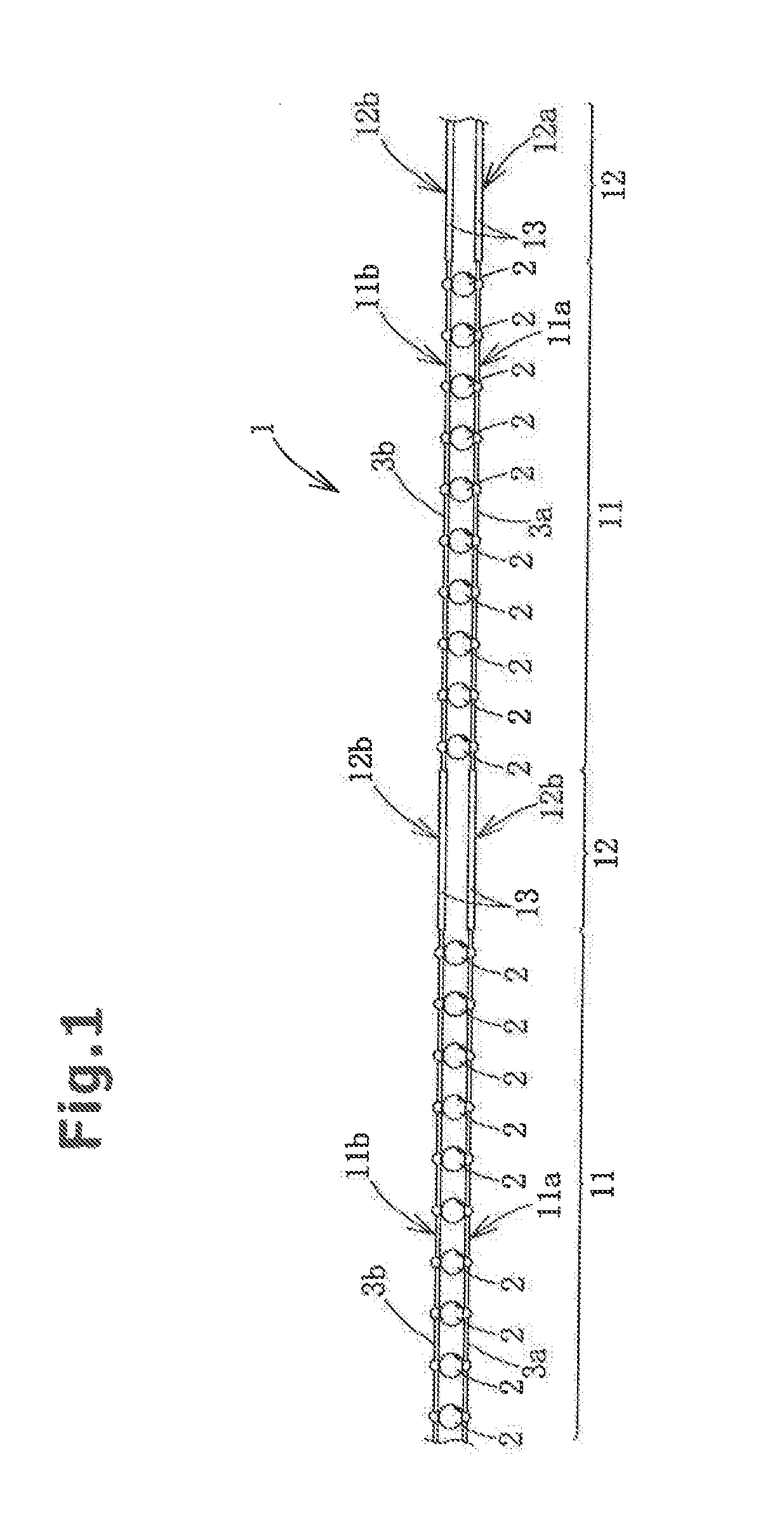

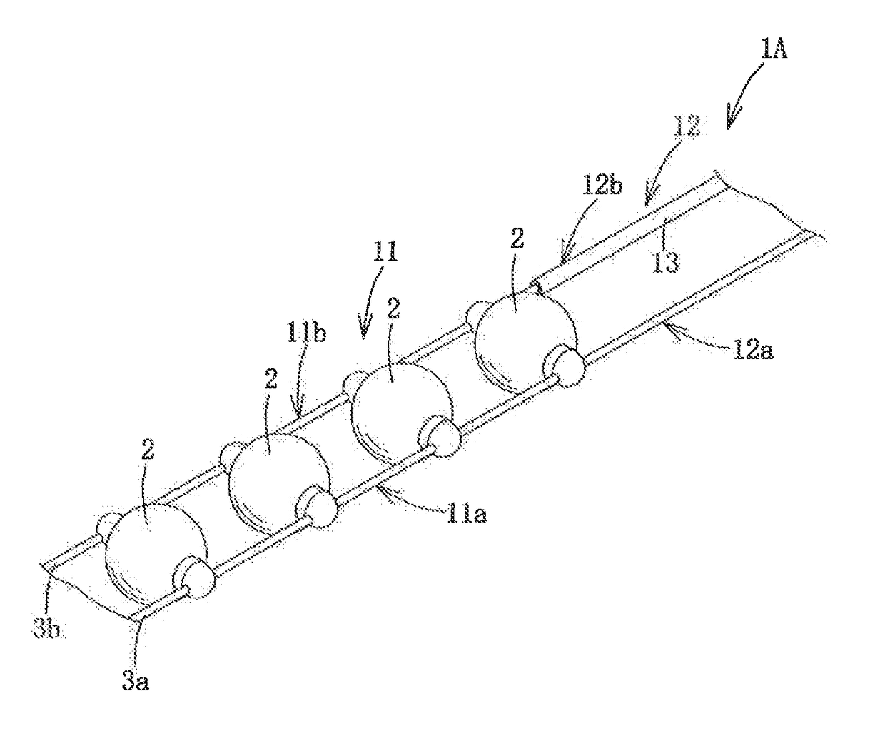
Image

  • Functional yarn equipped with semiconductor functional elements
  • Functional yarn equipped with semiconductor functional elements
  • Functional yarn equipped with semiconductor functional elements

Examples


Embodiment Construction

[0021]The present invention will now be described in detail on the basis of embodiments.

[0022]First, the overall construction of a functional yarn 1 equipped with semiconductor functional elements will be explained.

[0023]As shown in FIGS. 1 through 4, the functional yarn 1 equipped with semiconductor functional elements is made as a flexible cord, and comprises a plurality of semiconductor functional elements 2 that are formed as small granules having positive and negative electrodes 2a, 2b at opposite sides, and a pair of conducting wires 3a, 3b to which the plurality of semiconductor functional elements 2 are connected in parallel.

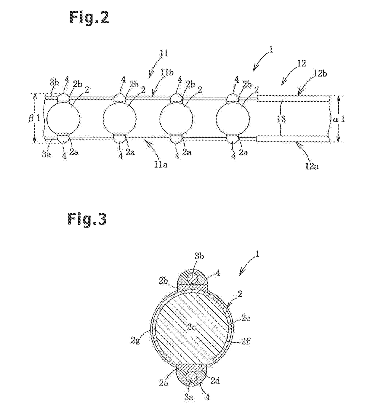
[0024]As shown in FIG. 3, the semiconductor functional elements 2 are built as spherical solar cells 2. In other words, each of the spherical solar cells 2 is manufactured by using a spherical p type silicon single crystal 2c of diameter 1.0 to 2.0 mm (in this embodiment, the diameter is 1.2 mm). A flat surface 2d is formed on one portion of the surface ...


PUM


Abstract

Functional yarn equipped with semiconductor functional elements includes: a plurality of semiconductor functional elements whose electrically conductive directions defined by positive and negative electrodes are aligned and disposed between a pair of conducting wires in which each of the positive electrodes being connected to the conducting wire and each of the negative electrodes being connected to the conducting wire; an element mounting region consisting of conducting wire portions on which a plurality of the semiconductor functional elements are disposed; a conducting wire region consisting of only conducting wire portions and an insulating member that covers the surface of at least one of the pair of conducting wire portions of the conducting wire region.

Description

BACKGROUND OF THE INVENTION[0001]The present invention relates to a functional yarn equipped with semiconductor functional elements, and in particular relates to such a functional yarn that includes a plurality of semiconductor functional elements which are formed as granules, and a pair of conducting wires that are flexible and to which the plurality of semiconductor functional elements are connected in parallel.[0002]In the prior art, in the field of manufactured textile products, a manufactured textile (i.e. a built-up mass made from textile) has been proposed to which are attached semiconductor functional elements of various types having a function of light reception or a function of light emission. In this type of manufactured textile with attached semiconductor functional elements, for example, functional yarns in the form of cords on which are mounted a plurality of semiconductor functional elements (solar cells, light emitting diodes, bypass diodes, or the like) are used as ...

Claims


Application Information

Patent Timeline
IPC IPC(8): H01L31/05H01L31/0224H01L31/0352
CPCH01L31/0504H01L31/022425H01L31/035281Y02E10/50H01L31/02002
Inventor NAKATA, JOSUKENAKAMURA, HIDETOSHIMASUDA, ATSUJITSUJI, TAKAHIROSASAGUCHI, NORIO
Owner SPHELAR POWER
Learn More