Semiconductor Device and Alternator Using Same

Active Publication Date: 2017-05-18
HITACHI POWER SEMICON DEVICE
View PDF7 Cites 1 Cited by
  • Summary
  • Abstract
  • Description
  • Claims
  • Application Information

AI Technical Summary

Benefits of technology

[0029]According to the present invention, it is possible to provide a semiconductor device that can be

Problems solved by technology

However, the technologies disclosed in above Patent Documents 1 to 3 have the following problems.
Accordingly, for example, for the use for the rectifying circuits of an alternator used for power generation of an automobile, it is necessary to manufacture a so-called forward (rectifying element S1) structure and a so-called reverse (rectifying element S2) structure, whose current directions are different, in respective different manufacturing processes, which causes a problem of requiring further improvement in the manufacturing equipment and cost.
Consequently, there is a problem that the above structures cannot be an appropriate structure at all, as a structure of a semiconductor device of a rectifying circuit or the like,

Method used


Image

  • Semiconductor Device and Alternator Using Same
  • Semiconductor Device and Alternator Using Same
  • Semiconductor Device and Alternator Using Same

Examples


Example

First Embodiment

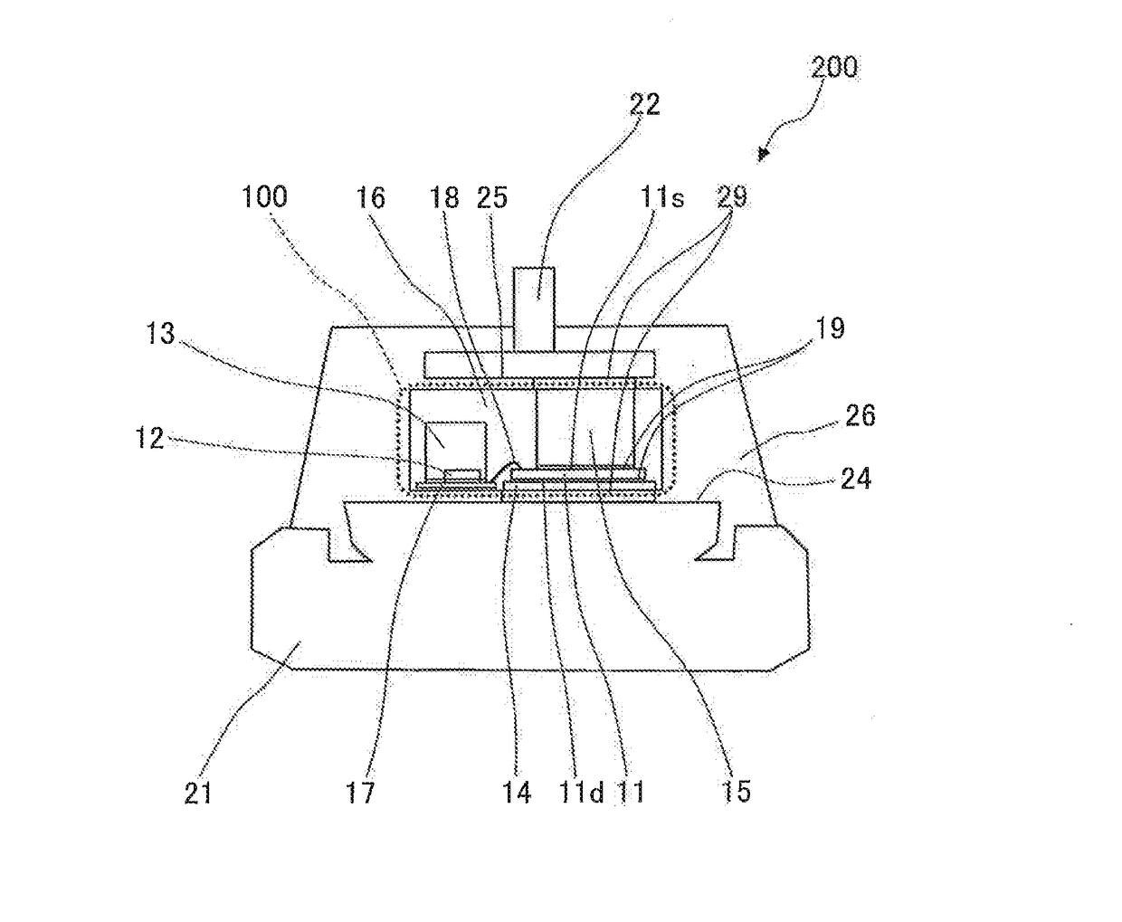
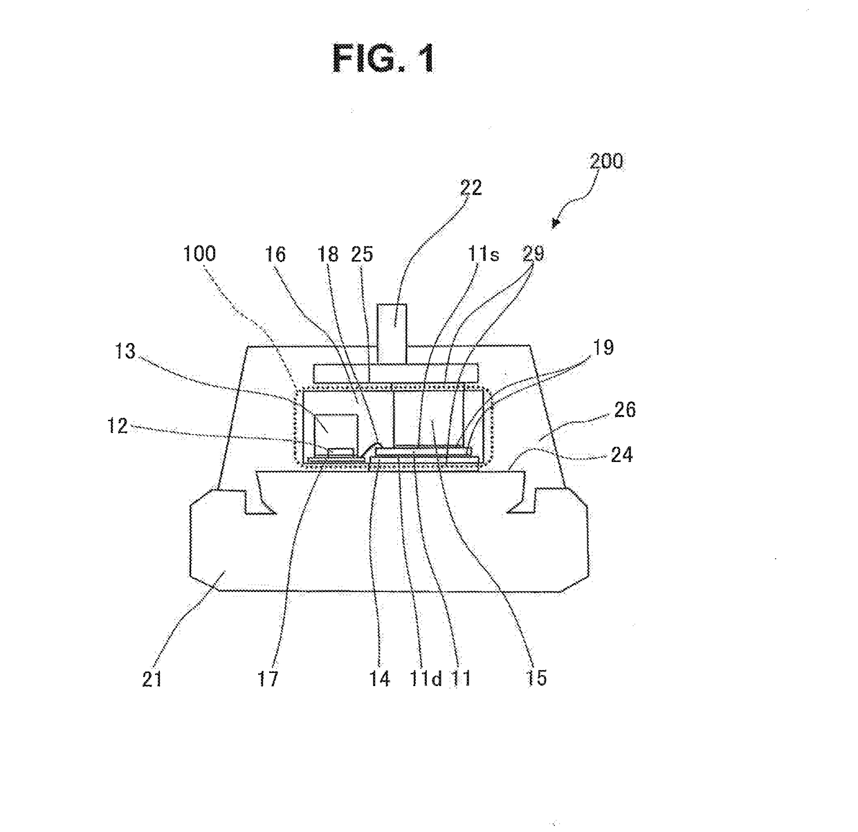
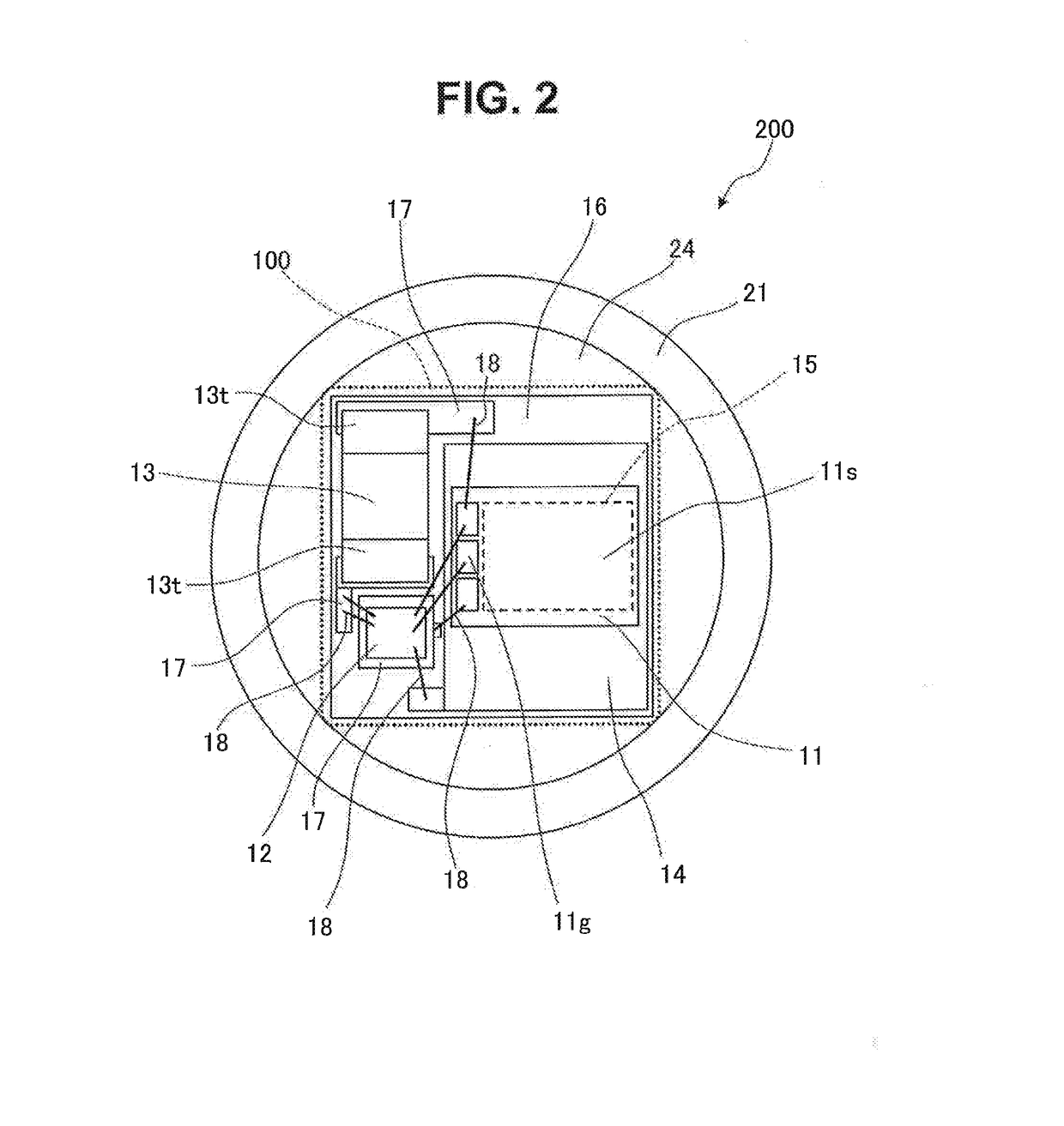
[0041]A semiconductor device (rectifying element) 200 in the first embodiment according to the present invention will be described, referring to FIG. 1 and FIG. 2.

[0042]FIG. 1 is a schematic diagram showing the cross-section of the vertical structure of the semiconductor device 200 in the first embodiment according to the present invention.

[0043]FIG. 2 is a schematic diagram showing the planar structure of the semiconductor device 200 in the first embodiment according to the invention. Incidentally, in FIG. 2, for easy understanding, a lead (the second external electrode) 22, a lead header (the second electrode surface portion) 25, and a second resin 26, which are disposed at the upper portion of the semiconductor device 200, are not shown.

[0044]Incidentally, as the configuration (structure) of a rectifying element (semiconductor device), there are two configurations (structures) called ‘forward configuration’ and ‘reverse configuration’. The difference between these...

Example

Second Embodiment

[0117]The semiconductor device 300 in the second embodiment according to the present invention will be described below, referring to FIG. 7. Incidentally, the semiconductor device 300 in the second embodiment has a reverse structure.

[0118]FIG. 7 is a schematic diagram showing the cross-section of the vertical structure of the semiconductor device 300 in the second embodiment according to the invention.

[0119]In FIG. 7, the semiconductor device 300 is different from the semiconductor device 200 in FIG. 1 in the upper and lower direction and connection relationship in which a base 21 having a base seat 24 at its upper portion, a lead 22 having a lead header 25 at its lower portion, and an electronic circuit body 100 are provided. In other points, as elements and a structure common with those in the first embodiment are adopted, overlapping description will be omitted, as appropriate.

[0120]In the following, description will be made mainly on matters in which the (revers...


PUM


Abstract

Provided are a semiconductor device realized easily at low cost without requiring a complicated manufacturing process, and an alternator using the same. The semiconductor device includes a base having a base seat, a lead having a lead header, and an electronic circuit body, wherein the electronic circuit body is arranged between the base and the lead; the base seat is connected to a first surface of the electronic circuit body; the lead header is connected to a second surface of the electronic circuit body; the electronic circuit body is integrally covered by resin, including a transistor circuit chip having a switching element, a control circuit chip for controlling the switching element, a drain frame, and a source frame; either one of the drain frame and the source frame, and the base are connected; and the other one of the drain frame and the source frame, and the lead are connected.

Description

CROSS REFERENCE TO RELATED APPLICATION[0001]This application claims the priority of Japanese Patent Application No. 2015-225258, filed on Nov. 18, 2015, the entire specification, claims and drawings of which are incorporated herewith by reference.BACKGROUND OF THE INVENTION[0002]Field of the Invention[0003]The present invention relates to a semiconductor device and an alternator using the same.[0004]Description of the Related Arts[0005]Related arts of the present technical field are disclosed in Patent Documents 1 to 3.[0006]Patent Document 1 (JP 2015-116053 A) discloses technology for a semiconductor device, with description “[PROBLEM TO BE SOLVED] Presented are a semiconductor device, an alternator, and a power conversion device, which can be simply assembled and have a low loss. [SOLUTION] A semiconductor device S1 according to the present invention includes a first external electrode 101 having an outer circumferential portion 101s in a circular shape in a top view, the external...

Claims


Application Information

Patent Timeline
IPC IPC(8): H01L23/495H02K11/04H01L23/31
CPCH01L23/49568H01L23/49562H01L23/49575H02K11/046H01L23/49548H01L23/49589H01L23/3114H01L25/16H02M7/003H02K11/05H01L23/051H01L23/3135H01L2224/73265H01L2224/01
Inventor KAWANO, KENYAISHIMARU, TETSUYAKURITA, SHINICHITERAKAWA, TAKESHI
Owner HITACHI POWER SEMICON DEVICE
Why Eureka
Try Eureka