Semiconductor optical integrated device and method of manufacturing the same

Active Publication Date: 2017-05-25
FURUKAWA ELECTRIC CO LTD
View PDF1 Cites 0 Cited by
  • Summary
  • Abstract
  • Description
  • Claims
  • Application Information

AI Technical Summary

Benefits of technology

The patent text discusses the need for higher performance in semiconductor optical integrated devices for better optical communication and cost reduction. To meet this demand, the text explains different waveguide structures that are used in the same semiconductor device to integrate multiple optical devices. For example, a buried hetero structure waveguide structure is used for high current injection efficiency and a deep ridge waveguide is used for low bending loss. The technical effect is the improved performance of semiconductor optical integrated devices through the use of different waveguide structures for each function.

Problems solved by technology

However, when the buried hetero structure waveguide and the deep ridge waveguide are integrated using the conventional method, there is a problem that it is difficult to sufficiently exhibit the performance as the semiconductor optical integrated device since each optimal design is different between the buried hetero structure waveguide and the deep ridge waveguide.
That is, when the optimal design for the buried hetero structure waveguide is conducted in the same semiconductor optical integrated device, it is not the optimal design for the deep ridge waveguide so that the performance of the deep ridge waveguide is suppressed.
Conversely, when the optimal design for the deep ridge waveguide is conducted, it is not the optimal design for the buried hetero structure waveguide so that the performance of the buried hetero structure waveguide is suppressed.

Method used


Image

  • Semiconductor optical integrated device and method of manufacturing the same
  • Semiconductor optical integrated device and method of manufacturing the same
  • Semiconductor optical integrated device and method of manufacturing the same

Examples


first embodiment

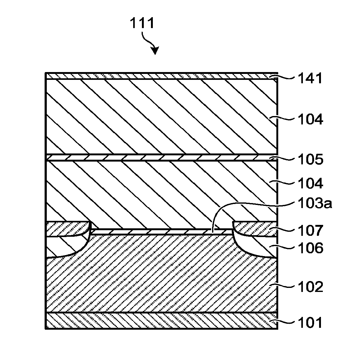
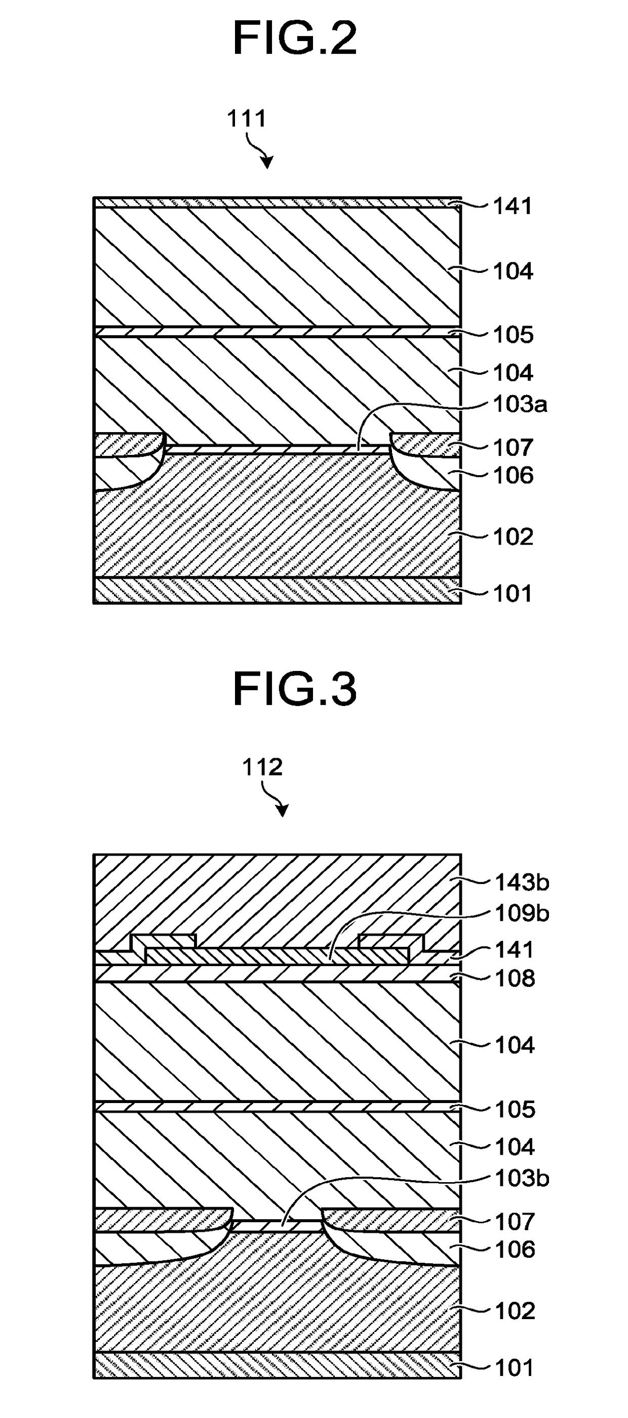
[0039]Planar Structure

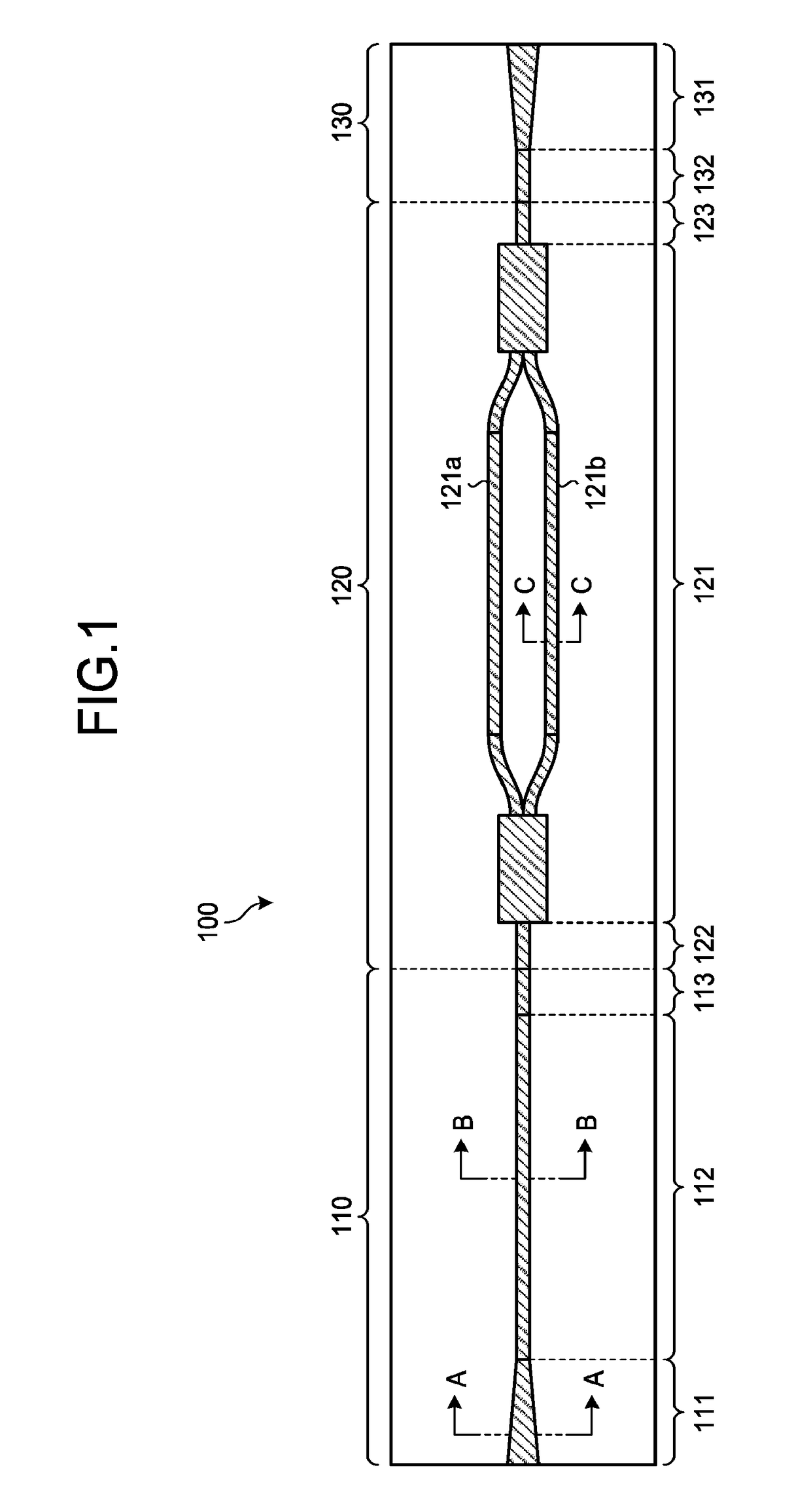
[0040]FIG. 1 is a schematic top view illustrating the semiconductor optical integrated device according to the first embodiment. Incidentally, the schematic top view illustrated in FIG. 1 illustrates only a waveguide and does not illustrate other components such as an electrode for simplification.

[0041]As illustrated in FIG. 1, a semiconductor optical integrated device 100 according to the first embodiment is provided with a buried hetero structure waveguide portion 110, a ridge waveguide portion 120, and a buried hetero structure waveguide portion 130. The buried hetero structure waveguide portions 110 and 130 are regions each of which has a waveguide in which semiconductor cladding materials are embedded near both sides of a waveguide core layer, and the ridge waveguide portion 120 is a region which has a waveguide in which a semiconductor layer including at least a waveguide core layer and an upper cladding layer protrudes in a mesa shape. Incidentally, the ...

second embodiment

[0128]Planar Structure

[0129]FIG. 15 is a schematic top view of the semiconductor optical integrated device according to the second embodiment. Incidentally, the schematic top view illustrated in FIG. 15 illustrates only a waveguide and does not illustrate other components such as an electrode for simplification.

[0130]As illustrated in FIG. 15, a semiconductor optical integrated device 200 according to the second embodiment is provided with a buried hetero structure waveguide portion 210, a ridge waveguide portion 220, and a buried hetero structure waveguide portion 230. The buried hetero structure waveguide portions 210 and 230 are regions each of which has a waveguide structure in which semiconductor cladding materials are embedded near both sides of a waveguide core layer, and the ridge waveguide portion 220 is a region which has a waveguide structure in which a semiconductor layer including at least a waveguide core layer and an upper cladding layer protrudes in a mesa shape. Inc...


PUM


Abstract

A semiconductor optical integrated device includes: a substrate; at least a lower cladding layer, a waveguide core layer, and an upper cladding layer sequentially layered on the substrate, a buried hetero structure waveguide portions each having a waveguide structure in which a semiconductor cladding material is embedded near each of both sides of the waveguide core layer; and a ridge waveguide portion having a waveguide structure in which a semiconductor layer including at least the upper cladding layer protrudes in a mesa shape. Further, a thickness of the upper cladding layer in each of the buried hetero structure waveguide portions is greater than a thickness of the upper cladding layer in the ridge waveguide portion.

Description

CROSS-REFERENCE TO RELATED APPLICATION(S)[0001]This application is a continuation of International Application No. PCT / JP2015 / 078161, filed on Oct. 5, 2015 which claims the benefit of priority of the prior Japanese Patent Application No. 2014-205739, filed on Oct. 6, 2014, the entire contents of which are incorporated herein by reference.BACKGROUND[0002]The present disclosure relates to a semiconductor optical integrated device and a method of manufacturing the same.[0003]Recently, a higher performance is required for a semiconductor optical integrated device from a viewpoint of advancement of optical communication and cost reduction. Further, in order to integrate a plurality of optical devices in a single semiconductor device, different waveguide structures suitable for each function of devices are used in the same semiconductor device (see, for example, Japanese Laid-open Patent Publication No. 2013-25242). For example, the different waveguide structures are used in the same semi...

Claims


Application Information

Patent Timeline
IPC IPC(8): G02B6/122G02B6/132G02F1/225H01S5/026H01S5/40G02B6/12G02B6/136H01S5/12
CPCG02B6/122G02B6/12011G02B6/12019G02B6/132G02B6/136G02F2001/212H01S5/4025G02F1/2257G02B2006/12121G02B2006/12142G02B2006/12097H01S5/0268G02F1/017G02F1/025H01S5/12H01S5/2232H01S5/3434H01S5/4012H01S5/4087H01S5/50G02F2201/063G02F2202/102H01S5/209G02B6/12004G02B6/1228G02B2006/12173G02F1/212G02B6/12
Inventor KIYOTA, KAZUAKIKIMOTO, TATSUYASAITO, YUSUKE
Owner FURUKAWA ELECTRIC CO LTD
Why Eureka
Try Eureka