Stable work function for narrow-pitch devices

a narrow-pitch, work function technology, applied in the direction of semiconductor devices, electrical apparatus, transistors, etc., can solve the problems of limiting the scaling factor of the device, the gate structure that allows oxygen diffusion into the gate dielectric can experience detrimental threshold voltage changes, and the scaling of the device is limited

Active Publication Date: 2017-05-25
TESSERA LLC
View PDF13 Cites 1 Cited by
  • Summary
  • Abstract
  • Description
  • Claims
  • Application Information

AI Technical Summary

Problems solved by technology

This can be a limiting factor in the reduction of the device size scaling.
In one example, a gate structure that permits oxygen diffusion into the gate dielectric can experience detrimental threshold voltage changes.
While finFETs and / or nanosheets can benefit from tight device-device spacing, these dimensions may limit scaling of these devices.
Further, devices requiring thicker dielectric for higher voltage operation are even more severely limited in the allowable dimensions.

Method used


Image

  • Stable work function for narrow-pitch devices
  • Stable work function for narrow-pitch devices
  • Stable work function for narrow-pitch devices

Examples


Embodiment Construction

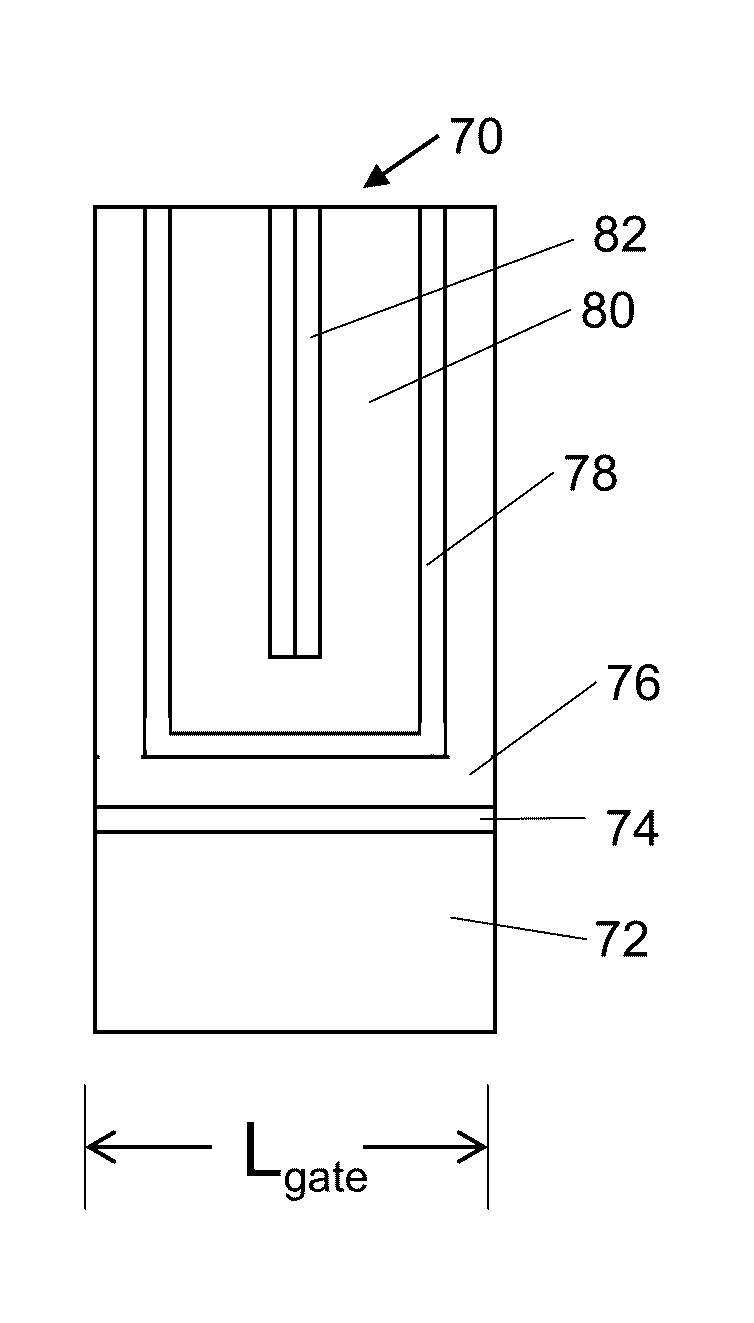
[0032]In accordance with the present principles, layer stacks are provided for formation between semiconductor structures in narrow gaps. A number of layers employed to effectively provide a diffusion barrier is reduced as well as a thickness of a barrier structure between the semiconductor structures. Conventional designs with a full stack of layers on each conducting interface limit the permissible spacing. The present principles open up these limitations to permit additional device scaling to further reduce device sizes.

[0033]In one embodiment, a work function setting metal stack of TiN / TiAlC / TiN is reduced to TiN / TiAlC or other oxygen absorbing materials by merging the TiAlC layers grown from two opposing regions. The merged TiAlC layer reduces the needed thickness of the work function setting metal stack, which permits further scaling of a gate width, fin spacing, nanosheet spacing, among other structures. By employing merged TiAlC, oxygen is absorbed more effectively permittin...


PUM

PropertyMeasurementUnit
thicknessaaaaaaaaaa
dielectric constantaaaaaaaaaa
widthaaaaaaaaaa

Abstract

A work function setting metal stack includes a configuration of layers including a high dielectric constant layer and a diffusion prevention layer formed on the high dielectric constant layer. An aluminum doped TiC layer has a thickness greater than 5 nm wherein the configuration of layers is employed between two regions as a diffusion barrier to prevent mass diffusion between the two regions.

Description

BACKGROUND[0001]Technical Field[0002]The present invention relates to semiconductor devices, and more particularly to devices and methods for fabricating such devices with work function setting metal layers, which are more compatible with narrower spaces between semiconductor regions.[0003]Description of the Related Art[0004]In nanometer scale devices, gate structures are often disposed between fin structures or other conducting structures, such as nanosheets. In many instances, the conducting or semiconducting structures are formed closer together due to scaling to smaller node technology sizes. This can be a limiting factor in the reduction of the device size scaling. With narrower gaps, it becomes more important to prevent oxygen diffusion between and into these narrow structures. In one example, a gate structure that permits oxygen diffusion into the gate dielectric can experience detrimental threshold voltage changes.[0005]While finFETs and / or nanosheets can benefit from tight ...

Claims


Application Information

Patent Timeline
Patent Type & Authority Applications(United States)
IPC IPC(8): H01L29/51H01L27/088
CPCH01L29/513H01L27/0886H01L29/517H01L29/4908H01L29/785H01L29/42392H01L29/78696H01L29/4966H01L21/823431H01L21/823437H01L21/02304H01L21/3205H01L21/022H01L29/42372H01L21/283H01L21/28088H01L29/0673H01L29/66742
Inventor ANDO, TAKASHIBAJAJ, MOHITHOOK, TERENCE B.PANDEY, RAJAN K.SATHIYANARAYANAN, RAJESH
Owner TESSERA LLC
Why Eureka
Try Eureka