Liquid crystal display device and display device substrate

a display device and liquid crystal technology, applied in the direction of instruments, computing, electric digital data processing, etc., can solve the problems of difficult to avoid the increase in the thickness of the entire display device, and the inability to adjust the display device. , to achieve the effect of high visibility, precise touch sensing function, and high visibility

Active Publication Date: 2017-06-01
TOPPAN PRINTING CO LTD
View PDF6 Cites 12 Cited by
  • Summary
  • Abstract
  • Description
  • Claims
  • Application Information

AI Technical Summary

Benefits of technology

[0056]According to the above-described aspects of the present invention, a liquid crystal display device can be provided in which a component having a thickness of such a touch panel is not used, a black layer is included, high visibility is obtained, high definition display of 300 ppi or more is possible, and precise touch sensing function is provided. Further, according to the above-described aspect of the present invention, a display device substrate having high visibility can be provided, which is used for a display device having a precise touch sensing function.
[0057]Further, according to the above-described aspects of the present invention, a display device substrate provided with a color filter layer, having high visibility can be provided, which is used for

Problems solved by technology

However, with a configuration of a display device provided with a touch panel, the thickness or weight of the entire display device increases.
Hence, in the configuration of such a display device, the touch panel may be an undesirable component.
Even with such a touch panel, it is difficult to avoid increase in the thickness of the entire display device.
Further, the display device provided with the above-described

Method used


Image

  • Liquid crystal display device and display device substrate
  • Liquid crystal display device and display device substrate
  • Liquid crystal display device and display device substrate

Examples


first embodiment

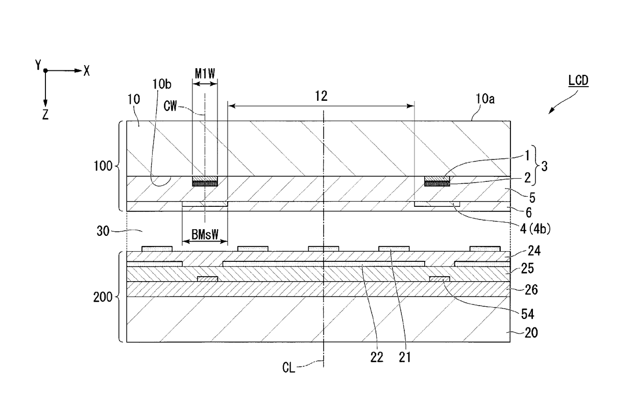
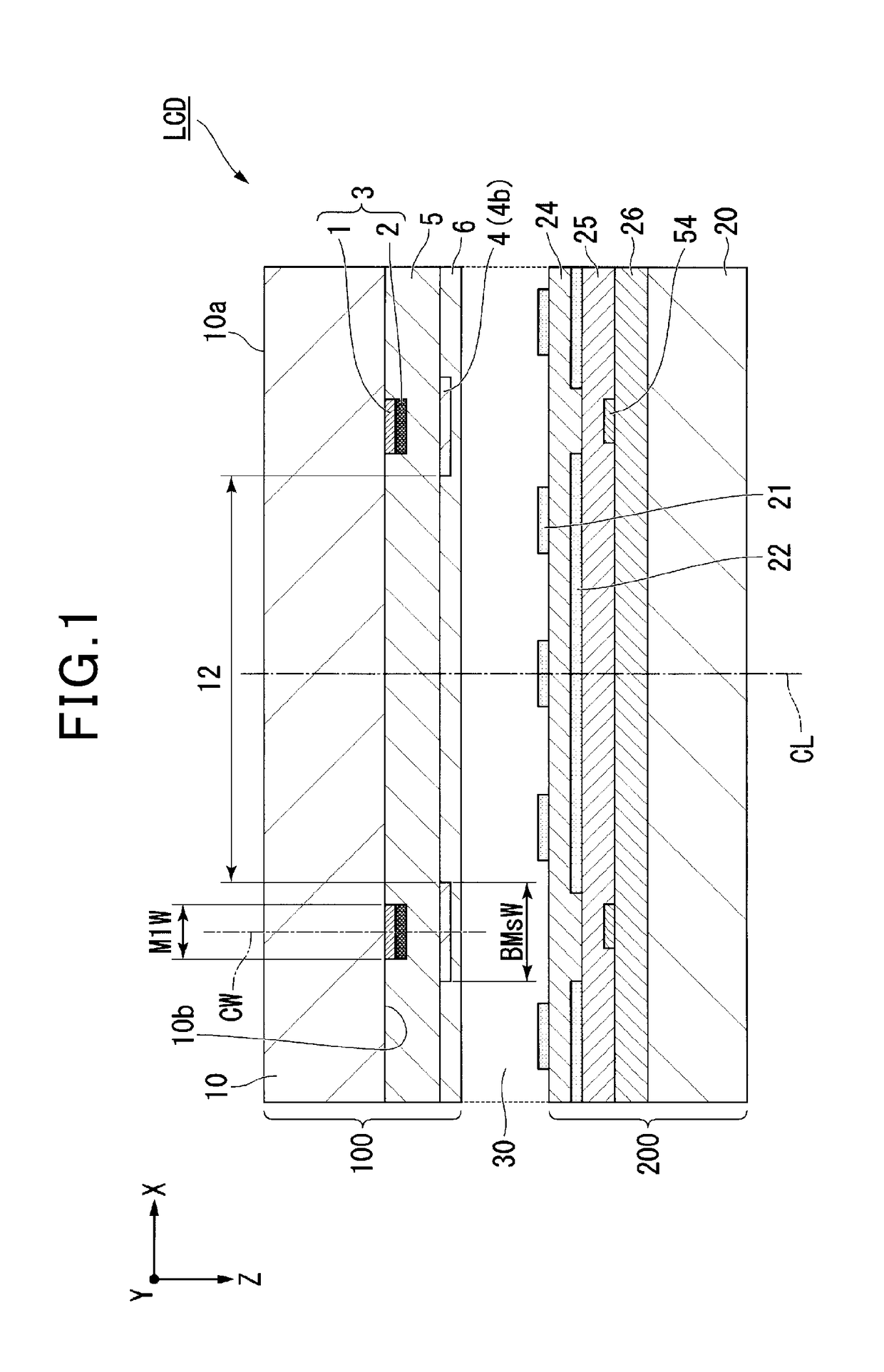
[0082]With reference to FIGS. 1 to 9, a liquid crystal display device according to a first embodiment will be described. A liquid crystal display device described in the present embodiment is provided with a display device substrate according to an embodiment of the present invention. It should be noted that ‘plan view’ mentioned in the following description refers to a plane as viewed from a direction of an observer's observing a display surface (plane of display device substrate) of the liquid crystal display device. A shape of the display portion or a shape of the opening defining a pixel of the liquid crystal display device according to the embodiment of the present invention, and the number of pixels composing the liquid crystal display device are not limited. However, in the embodiment specifically described below, the liquid crystal display device will be described, defining, in plan view, a short side direction of the pixel as an X-direction, a long side direction of the pix...

second embodiment

[0170]With reference to FIG. 10, hereinafter will be described a display device substrate according to a second embodiment of the present invention. In the second embodiment, the like reference signs are designated to the like components of the first embodiment to omit or simplify description.

[0171]FIG. 10 is a cross-sectional view showing a part of a display device substrate of the present invention.

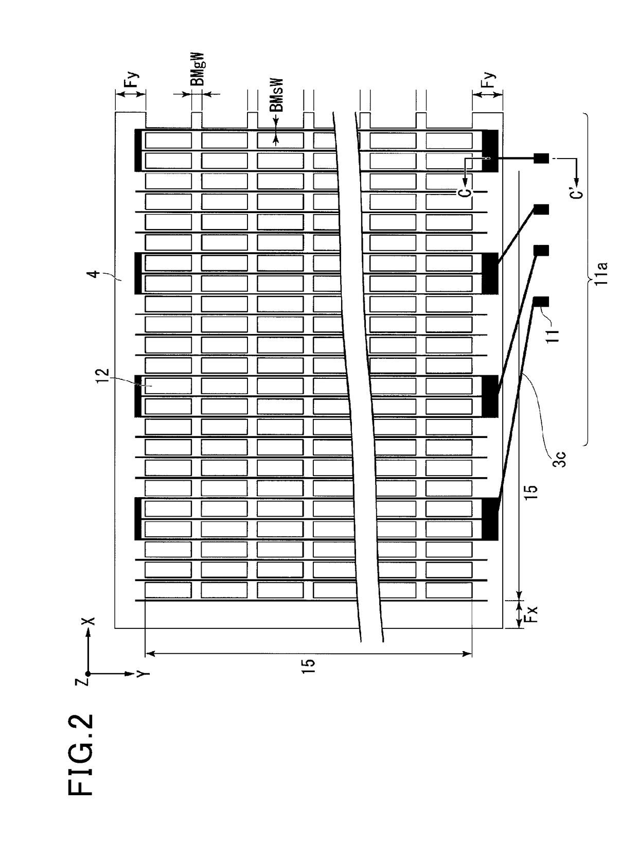
[0172]The display device substrate according to the second embodiment includes a laminate structure composed of the black layer 1 and the first metal layer 2, a first wiring layer 3 disposed on the transparent substrate 10, a black matrix 4′ provided on the transparent substrate 10 so as to cover the side surface and the surface of the first wiring layer 3, and a transparent resin layer 6 provided on the transparent substrate 10 so as to cover the black matrix 4′. The black matrix 4′ has a plurality of openings 12 in the effective display region 15. With this configuration, to avoid an ...

third embodiment

[0173]With reference to FIGS. 11 to 13, hereinafter will be described a display device substrate and a liquid crystal display device according to a third embodiment of the present invention. According to the third embodiment, the like reference signs are designated to the like components of the first and second embodiments to omit or simplify description.

[0174]FIG. 12 is a cross-sectional view showing a part of a display device substrate 100A according to the third embodiment of the present invention. The display device substrate 100A is used for a liquid crystal display device LCD′ shown in FIG. 11. In the display device substrate 100A, the first wiring layer 3, a color filter CF (color filter layer), a transparent resin layer 5, a black matrix 4 and the transparent resin layer 6 are formed on the transparent substrate 10 in this order. In other words, the color filter CF is disposed between the first metal layer 2 and the transparent resin layer 5. In the color filter CF, a colore...


PUM


Abstract

A liquid crystal display device including: a counter substrate having a first transparent substrate, a laminate structure of a black layer and a first metal layer, and a plurality of terminal portions; a liquid crystal layer; an array substrate having a second transparent substrate, an active element, a second wiring layer formed of a second metal layer, and a light shielding layer. The counter substrate has the first wiring layer, a black matrix, and a first transparent resin layer laminated in this order. The black matrix has a line width larger than a line width (M1W) of the first wiring layer, overlapping the first wiring layer so as to include a pattern of the first wiring layer. The active element is covered with a light shielding pattern via a first insulation layer. A change in electrostatic capacitance produced between the first wiring layer and the second wiring layer is detected.

Description

CROSS-REFERENCE TO RELATED PATENT APPLICATION[0001]This application is a continuation application filed under 35 U.S.C. §111(a) claiming the benefit under 35 U.S.C. §§120 and 365(c) of International Application No. PCT / JP2014 / 073513, filed on Sep. 5, 2014, the entirety of which is hereby incorporated by reference.TECHNICAL FIELD[0002]The present invention relates to a liquid crystal display device provided with a low-resistive wiring pattern, improving visibility thereof, and capable of reducing noise produced by active elements. The present invention relates to an in-cell type liquid crystal display device in which an electrostatic capacitive type touch sensing function is integrated with the liquid crystal cell.BACKGROUND[0003]In a generally known configuration, a touch panel is provided on a surface of a display device included in portable equipment such as smartphones or tablet computers. The touch panel is used as an input means for detecting a contact between a finger or a poi...

Claims


Application Information

Patent Timeline
IPC IPC(8): G06F3/041G02F1/1362G06F3/047G02F1/1335G02F1/1333G02F1/1343G06F3/044G02F1/1368
CPCG06F3/0418G02F2001/134372G02F1/136286G02F1/1368G02F1/133512G02F1/133345G02F1/133514G02F1/134363G02F1/13338G06F3/0412G06F3/047G02F2001/136295G02F2001/13629G02F2201/123G02F2201/121G06F3/044G02F1/133509G02F1/133602G06F3/04184G06F3/0445G06F3/0446G02F1/133614G02F1/134372G02F1/1333G02F1/1335G02F1/13629G02F1/136295
Inventor KIMURA, YUKIHIROFUKUYOSHI, KENZO
Owner TOPPAN PRINTING CO LTD
Why Eureka
Try Eureka