

Thin film transistor substrate for organic light-emitting diode display and manufacturing method thereof
- Summary
- Abstract
- Description
- Claims
- Application Information
AI Technical Summary
Benefits of technology
Problems solved by technology
Method used
Image

Examples
Embodiment Construction
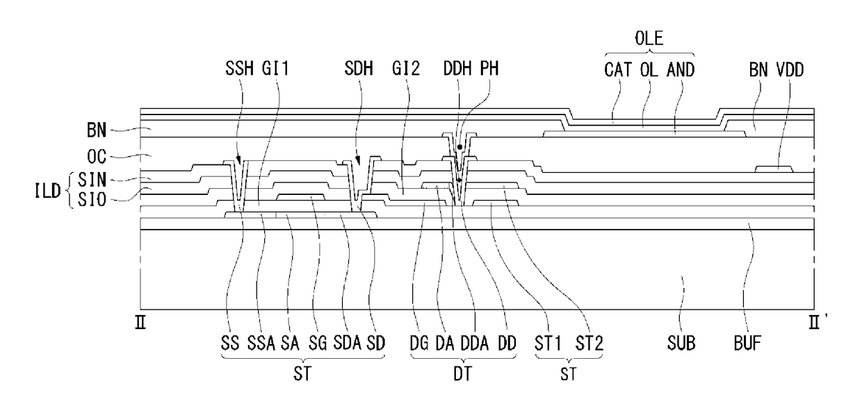
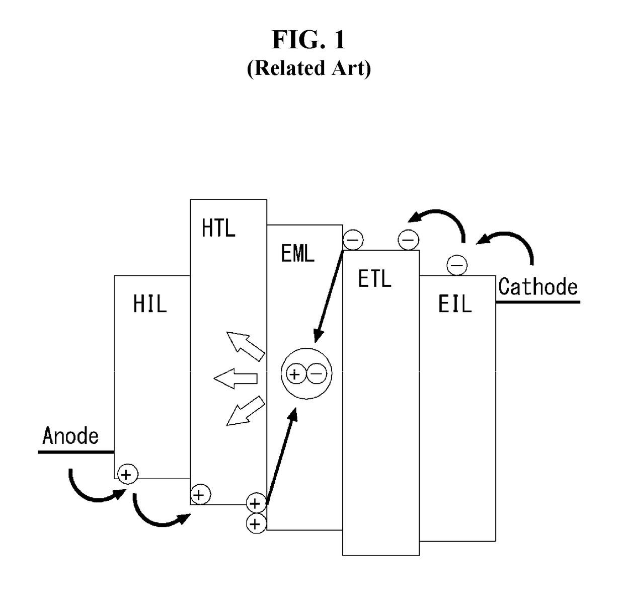
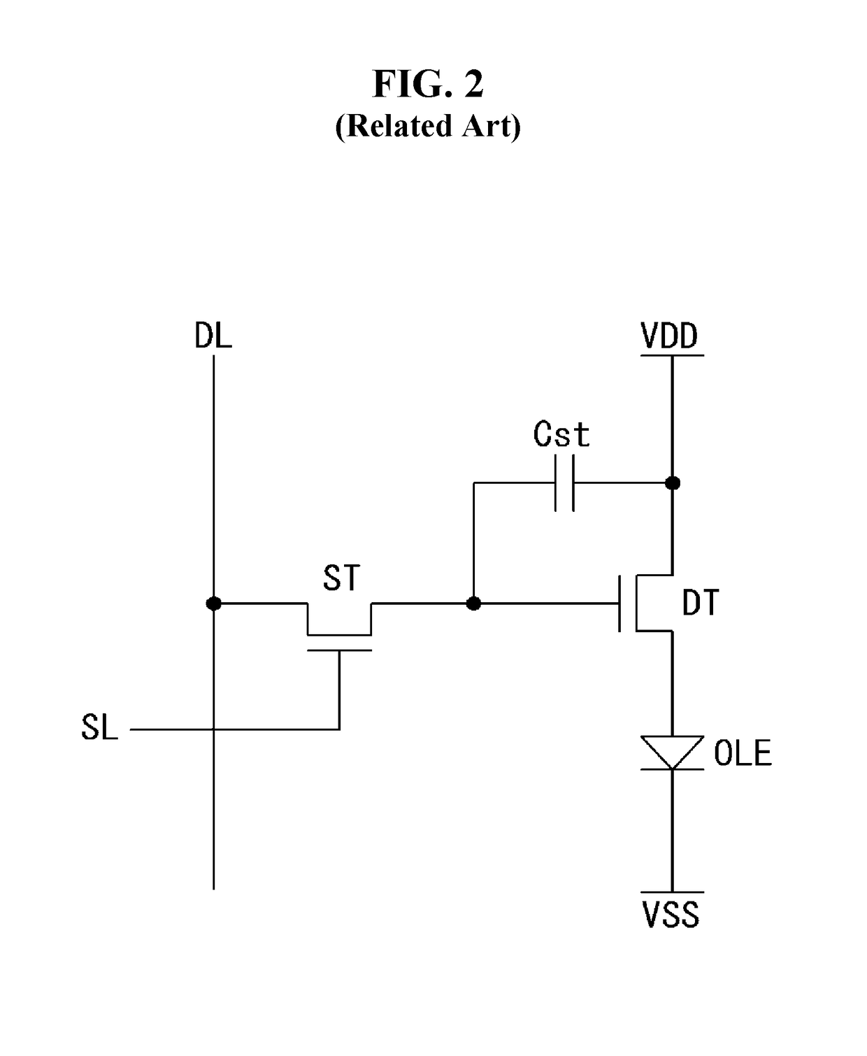
[0037]Reference will now be made in detail to embodiments of the present disclosure, examples of which are illustrated in the accompanying drawings. In the following description, when a detailed description of well-known functions or configurations related to this document is determined to unnecessarily cloud a gist of the invention, the detailed description thereof will be omitted. The progression of processing steps and / or operations described is an example; however, the sequence of steps and / or operations is not limited to that set forth herein and may be changed as is known in the art, with the exception of steps and / or operations necessarily occurring in a certain order. Like reference numerals designate like elements throughout. Names of the respective elements used in the following explanations are selected only for convenience of writing the specification and may be thus different from those used in actual products.
[0038]In the description of embodiments, when a structure is...
PUM
 Abstract
Description
Claims
Application Information