Semiconductor Devices with Integrated Thin-Film Transistor Circuitry

a technology of integrated thin-film transistors and semiconductor devices, which is applied in the direction of semiconductor devices, semiconductor/solid-state device details, electrical apparatuses, etc., can solve the problems of limited battery operation time, low light efficiency, and high power consumption

Active Publication Date: 2017-06-22
JADE BIRD DISPLAY SHANG HAI LTD
View PDF16 Cites 92 Cited by
  • Summary
  • Abstract
  • Description
  • Claims
  • Application Information

AI Technical Summary

Problems solved by technology

However, conventional TFT-LCD displays and TFT-OLED displays suffer from low light efficiency, causing high power consumption and limited battery operation time.
However, in active matrix LED displays, combi...

Method used


Image

  • Semiconductor Devices with Integrated Thin-Film Transistor Circuitry
  • Semiconductor Devices with Integrated Thin-Film Transistor Circuitry
  • Semiconductor Devices with Integrated Thin-Film Transistor Circuitry

Examples


Embodiment Construction

[0022]The figures and the following description relate to preferred embodiments by way of illustration only. It should be noted that from the following discussion, alternative embodiments of the structures and methods disclosed herein will be readily recognized as viable alternatives that may be employed without departing from the principles of what is claimed.

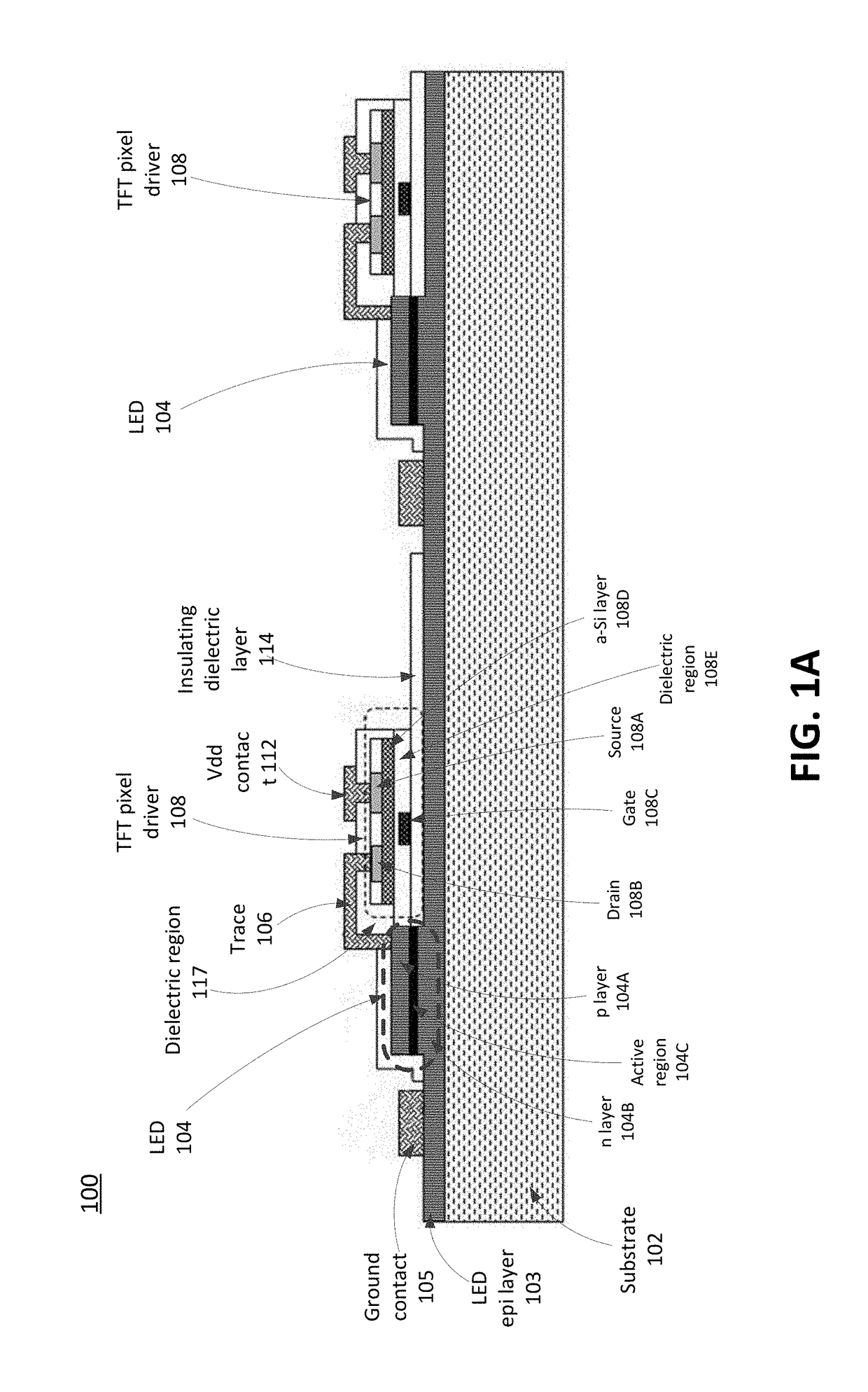
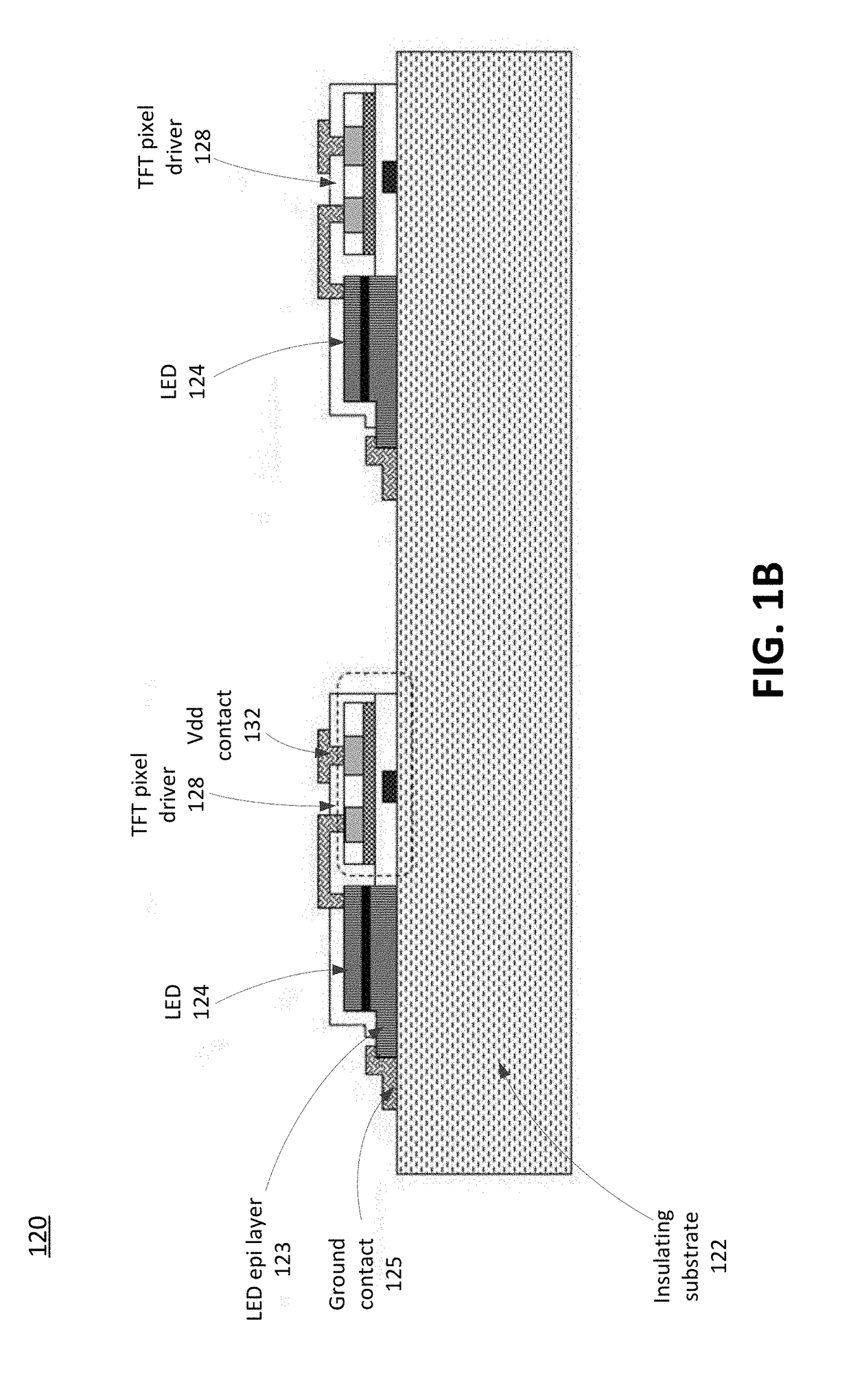
[0023]FIG. 1A is a cross-sectional view of one example of a display panel 100 with TFT pixel drivers 108 integrated with LEDs 104 on an LED die. In FIG. 1A, an array of LEDs 104 is first epitaxially grown on a substrate 102, forming an LED wafer (or a wafer containing multiple LED dies). The TFT driver circuitry, which is an array of TFT pixel drivers 108, is then directly fabricated on the LED wafer. In this example, the TFT pixel driver 108 is a bottom gate TFT transistor and an insulating dielectric layer 114 separates the bottom gate 108C from the underlying substrate 102.

[0024]For clarity, FIG. 1A shows only two LEDs 104 ...


PUM


Abstract

Various embodiments include a semiconductor device with thin-film transistor (TFT) circuitry monolithically integrated with other non-TFT functional devices. One example is an integrated LED display panel, in which an array of LEDs is integrated with corresponding TFT driver circuitry. The TFT driver circuitry typically is an array of pixel drivers that drive the LEDs.

Description

CROSS-REFERENCE TO RELATED APPLICATION(S)[0001]This application claims priority under 35 U.S.C. §119(e) to U.S. Provisional Patent Application Ser. No. 62 / 270,375, “Monolithically Integrated TFT Driven LED Array Display Panels and Methods of Making Such,” filed Dec. 21, 2015. The subject matter of all of the foregoing is incorporated herein by reference in their entirety.BACKGROUND[0002]1. Field of the Invention[0003]This disclosure relates generally to semiconductor devices with integrated thin-film transistor (TFT) circuitry, for example displays with epitaxially grown light emitting diodes (LEDs) integrated with corresponding TFT pixel drivers.[0004]2. Description of Related Art[0005]Active matrix liquid-crystal displays and organic light emitting diode (OLED) displays combined with thin-film transistor technology are becoming increasingly popular in today's commercial electronic devices. These displays are widely used in laptop personal computers, smartphones and personal digita...

Claims


Application Information

Patent Timeline
IPC IPC(8): H01L27/15H01L23/00H01L23/29H01L25/16H01L27/12
CPCH01L27/156H01L25/16H01L27/1255H01L23/29H01L2224/73253H01L2924/12041H01L2924/13069H01L2924/1431H01L2924/1426H01L24/73H01L25/167H01L25/50H01L25/0753H01L2224/24137H01L2224/24998H01L2224/24011H01L2224/245H01L24/16H01L24/24H01L2224/16237H01L2924/00014H01L25/075
Inventor ZHANG, LEIOU, FANGLI, QIMING
Owner JADE BIRD DISPLAY SHANG HAI LTD
Why Eureka
Try Eureka